Understanding Printed Wiring Boards (PWBs) and Their Role in Modern Electronics
2025.01.21
In our increasingly technology-driven world, the silent workhorses behind countless electronic devices are printed wiring boards (PWBs). Often called the backbone of electronic systems, these boards act as a structured foundation, meticulously connecting components. This article demystifies the role of PWBs, outlining their crucial contribution to everything from smartphones to spacecraft, and distinguishes them from closely related PCBs.
What is a Printed Wiring Board (PWB)?
Printed Wiring Board
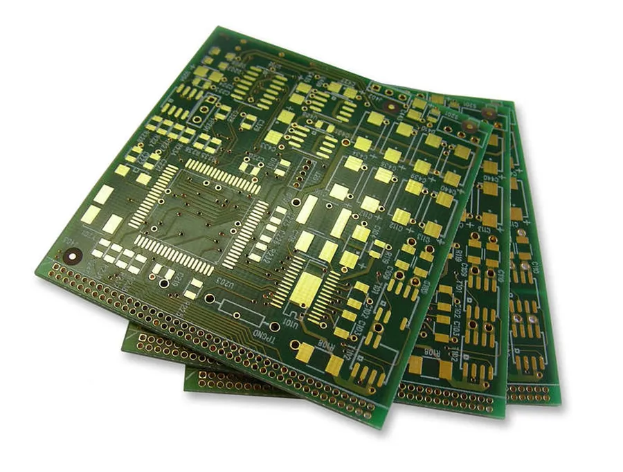
A Printed Wiring Board (PWB) serves as the foundational substrate in electronic devices, providing both physical support and electrical pathways for electronic components. It is the bare board, pre-populated with electronic parts, that establishes a robust platform for circuit construction. Essentially, it’s the 'skeleton' upon which all electronic circuitry is built.
The PWB is designed with conductive tracks, pads, and other features that facilitate the connection of components, prior to the actual placement and soldering of components. These features are typically made from copper and are formed using etching techniques on an insulating substrate.
PWB vs. PCB: Key Differences Explained
PCB and PWB Comparison
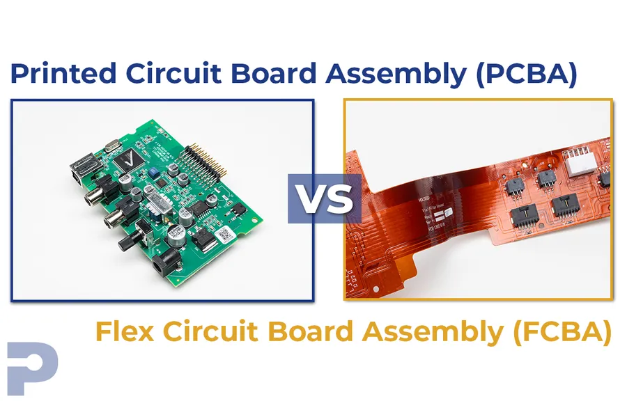
While the terms Printed Wiring Board (PWB) and Printed Circuit Board (PCB) are often used interchangeably, a subtle but significant distinction exists. Traditionally, a PWB refers to the bare substrate, the board itself before any electronic components are attached. Conversely, a PCB is the same board after components have been mounted and electrically connected. This distinction reflects the fabrication stage, where the PWB is the blank canvas, and the PCB is the completed functional assembly.
Feature
Printed Wiring Board (PWB)
Printed Circuit Board (PCB)
Components
No components mounted
Components mounted and electrically connected
Function
Provides physical support and electrical connections
Functional electronic assembly ready for use
Stage of Assembly
Bare substrate, before component mounting
Completed assembly with components
Typical Use
Intermediate product in PCB assembly process
Final product integrated into electronic devices
Synonym
Bare board
Loaded board or assembled board
In modern practice, the terms are frequently conflated. The industry shift means that 'PCB' is now often used to refer to both bare boards and fully assembled boards. However, understanding the original distinction is crucial for clear communication, especially in contexts involving manufacturing and assembly processes where each term still holds specific meanings. The ambiguity in modern usage means it is essential to clarify the context to avoid misunderstanding.
Evolution of Printed Wiring Board Technology
Vintage Printed Wiring Board
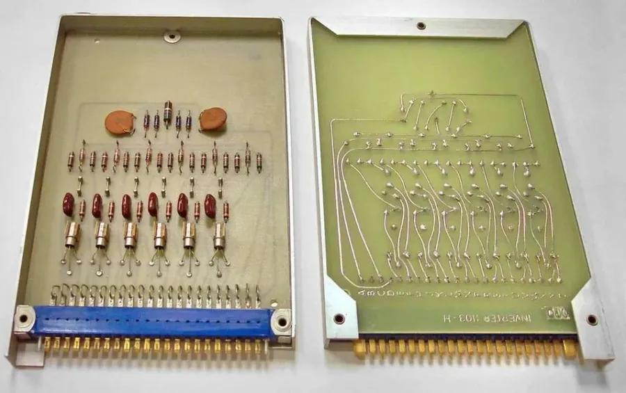
The evolution of Printed Wiring Board (PWB) technology is a story of continuous innovation driven by the relentless pursuit of smaller, faster, and more reliable electronics. From their humble beginnings as simple single-sided boards to today's complex multilayered designs, PWBs have been at the forefront of electronic advancement, enabling the miniaturization and increased performance of devices.
Early Single-Sided Boards The initial PWBs were single-sided, consisting of a conductive layer (typically copper) laminated onto one side of an insulating substrate. These boards were suitable for simple electronic circuits, but their limited routing capacity restricted the complexity of designs.
Double-Sided Boards The development of double-sided boards, with conductive layers on both sides of the substrate, significantly increased routing flexibility and component density. This innovation allowed for more complex circuits and smaller form factors.
Multilayer Boards Multilayer boards, incorporating multiple conductive layers within the substrate, marked a major leap forward. These boards facilitated highly complex designs, enabling dense interconnections and improved signal integrity. The number of layers ranges from four to over fifty, accommodating intricate electronics.
Advanced Materials The move from materials like phenolic and paper-based laminates to more advanced materials such as FR-4 (Flame Retardant 4), polyimide, and metal-core substrates has enabled PWBs to operate at higher temperatures, frequencies, and in more demanding environments. These materials offer superior thermal, electrical, and mechanical properties.
Surface Mount Technology (SMT) The development of surface mount technology (SMT), which allowed components to be directly mounted on the surface of the board without the need for through-hole leads, further accelerated miniaturization and automated assembly processes, enhancing both efficiency and component density.
High-Density Interconnect (HDI) Technology HDI technology, characterized by finer lines, smaller vias, and increased layer counts, allows for extremely dense component placement and routing, crucial for compact and high-performance devices. This technology continues to push the boundaries of miniaturization.
Technology
Key Features
Impact on Electronics
Single-Sided PWBs
One conductive layer
Basic, limited complexity
Double-Sided PWBs
Two conductive layers
Increased routing flexibility
Multilayer PWBs
Multiple conductive layers
Complex, dense interconnections
Advanced Materials (FR-4, polyimide)
Enhanced thermal and electrical properties
Improved performance and reliability
Surface Mount Technology (SMT)
Surface-mounted components
Miniaturization and automated assembly
High-Density Interconnect (HDI)
Finer lines, smaller vias
Extremely dense component placement
The Manufacturing Process of PWBs
PWB Manufacturing
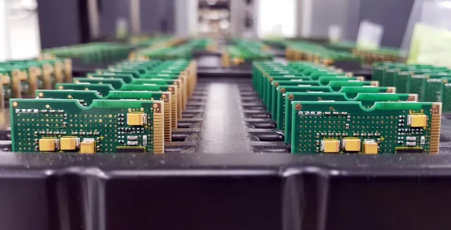
The fabrication of Printed Wiring Boards (PWBs) is a sophisticated multi-stage process that transforms raw materials into the foundational elements of electronic devices. This process involves meticulous design, precise chemical treatments, and stringent quality control measures to ensure the reliability and performance of the final product.
Design and Preparation The process begins with a detailed circuit design using specialized software (e.g., CAD). This design is then converted into a set of manufacturing files, including Gerber files. These files dictate the precise layout of the conductive tracks, pads, and other features on the PWB.
Material Selection Appropriate raw materials are chosen based on the performance requirements of the final application. This typically involves selecting the base substrate material (e.g., FR-4, polyimide) and copper foil that will form the conductive layers.
Layer Imaging and Patterning For multilayer PWBs, each layer's design is transferred onto the copper foil using a photo-imaging process. This involves coating the copper with a photoresist material, exposing it to UV light through a photomask (film or direct laser imaging), and then removing the unexposed photoresist and copper through etching, and then the remaining photoresist is removed, leaving the desired copper pattern.
Drilling Next, holes are drilled into the board with extreme precision. These holes are used for through-hole components and vias, which establish electrical connections between different layers of the PWB. Computer-numerical-control (CNC) machines use high-precision drills to ensure accuracy.
Electroless and Electrolytic Plating To make the drilled holes conductive and to increase the copper thickness, an electroless plating process is used, in which a thin copper coating is chemically deposited in the holes and on the PWB surface. Then, using an electroplating process, the copper thickness is increased to specified dimensions.
Layer Lamination For multi-layer PWBs, the different patterned layers are precisely aligned and then fused together using a combination of heat and pressure and a bonding agent, such as epoxy resin prepreg. This process creates a solid, unified structure with layers accurately positioned.
Solder Mask Application A solder mask layer, a protective coating made of polymer material, is applied to the outer layers of the PWB, which prevents solder bridges during component assembly. This layer is also used as a protective layer.
Silkscreen Application A silkscreen layer is added to the PWB, typically using white ink. This layer contains important component placement information, logos, and other markings.
Surface Finish The PWB undergoes a surface finishing process to protect the exposed copper pads and enhance solderability. Common finishes include hot air solder leveling (HASL), electroless nickel immersion gold (ENIG), and organic solderability preservatives (OSP).
Electrical Testing Each PWB undergoes rigorous electrical testing to ensure that every circuit connection is correct and meets performance requirements. This may involve using a flying probe tester or a bed of nails fixture to identify shorts, opens, and other electrical faults.
Profiling and Final Inspection The PWB is cut from the larger panel to its specific shape using routing machines. Then, a final visual inspection is performed to check for surface flaws, proper dimensions, and that the overall quality of the PWB is up to standard before being packed and shipped.
Materials Used in Printed Wiring Boards
PWB Materials
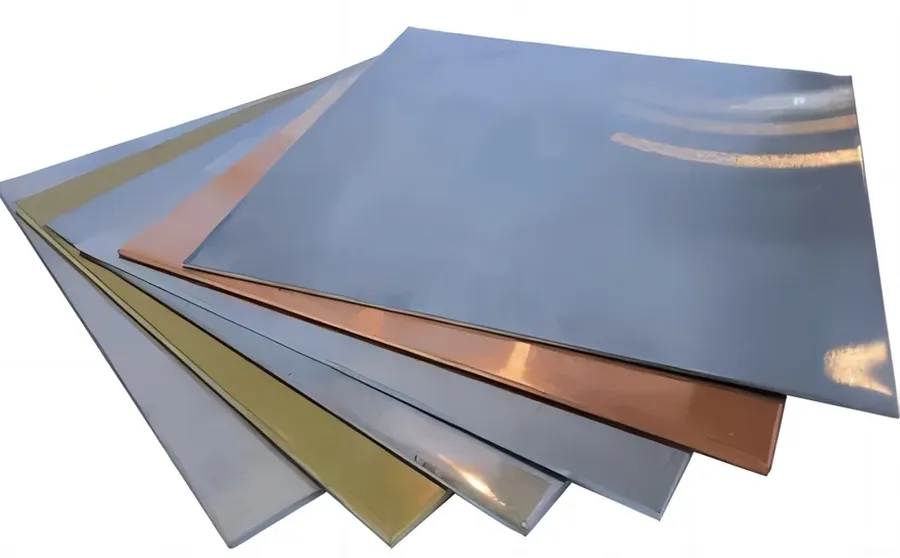
The performance and reliability of a Printed Wiring Board (PWB) are significantly influenced by the materials from which it is constructed. These materials provide the necessary structural support, electrical insulation, and thermal management properties for the electronic components mounted on them. The selection of materials is a crucial aspect of PWB design and fabrication, tailored to meet specific application requirements.
Material
Description
Key Characteristics
Common Applications
FR-4
A composite material made of woven fiberglass cloth with an epoxy resin binder.
Good electrical insulation, high strength-to-weight ratio, cost-effective, widely available.
General-purpose electronics, consumer devices, most standard PCBs.
Polyimide
A high-performance polymer known for its exceptional thermal stability and flexibility.
Excellent heat resistance, dimensional stability, good chemical resistance, flexible.
RF and microwave applications, high-speed digital circuits, telecommunications
Teflon (PTFE)
Polytetrafluoroethylene based material known for its inertness and dielectric properties
Extremely low loss, very low dielectric constant, high-temperature capabilities
High-frequency and high-performance applications, aerospace
CEM-1, CEM-3
Composite materials similar to FR-4 but with a paper or non-woven glass core.
More affordable alternative to FR-4 with slightly less performance.
General applications, less demanding projects
Dielectric Constant Considerations The dielectric constant of the material impacts the electrical signal propagation speed and impedance characteristics. Materials with a lower dielectric constant are generally preferred for high-speed applications to minimize signal distortion and losses.
Thermal Management Materials with good thermal conductivity, like metal cores, are used to efficiently dissipate heat, preventing overheating and ensuring the reliability of high-power components.
Flexibility Flexible materials such as polyimide enable the production of PWBs that can conform to non-planar surfaces and withstand dynamic bending and flexing in flexible electronic applications.
Environmental Factors Material selection should consider the environmental conditions in which the PWB will operate, such as temperature ranges, humidity levels, and exposure to chemicals. Materials with high environmental stability are required for harsh environments.
Regulatory Compliance Materials must comply with environmental regulations like RoHS and REACH, which restrict the use of hazardous substances.
Printed Wiring Board Design Considerations
Effective Printed Wiring Board (PWB) design is critical for ensuring optimal electrical performance and signal integrity. This involves careful consideration of several key parameters, including trace widths, impedance control, layer stacking, and routing strategies. These factors directly impact the functionality, reliability, and manufacturability of the final electronic product.
Design Parameter
Description
Impact on Performance
Trace Widths
The width of conductive traces on the PWB. Wider traces have lower resistance.
Determines current-carrying capacity and impedance.
Impedance Control
Managing the characteristic impedance of signal traces. A controlled impedance ensures minimal signal reflections.
Essential for high-speed signal integrity.
Layer Stacking
The arrangement of conductive and insulating layers in a multilayer PWB.
Impacts signal routing, EMI, and power distribution.
Routing Strategies
Methods used to route signal traces, including via placement, and minimizing signal path length.
Reduces signal delay and crosstalk.
Trace Width and Spacing The width of copper traces should be calculated based on the required current carrying capacity and thermal management considerations. Minimum spacing between traces must adhere to design rules based on the manufacturing process to avoid electrical shorts. IPC-2221 standards provide guidelines for determining trace widths and spacing.
Impedance Matching Controlled impedance traces are crucial for high-speed signal transmission. This involves calculating trace width and spacing in relation to the substrate material to achieve the desired characteristic impedance (e.g., 50 ohms). Impedance mismatching causes signal reflections and signal loss.
Layer Stackup Optimization The sequence of layers in a multilayer PWB significantly affects signal routing, power distribution, and electromagnetic compatibility (EMC). Proper power and ground plane placement minimizes noise and ensures stable power delivery. Signal layers should be placed to reduce cross-talk. The use of signal layers between power/ground planes to reduce emissions.
Routing Techniques Effective signal routing includes keeping signal paths short, minimizing vias, and avoiding 90 degree angles that can cause signal reflections. Differential pair routing should also be used to minimize noise and interference when routing pairs of signals, while also controlling impedance.
Applications of Printed Wiring Boards Across Industries
Automotive PWB
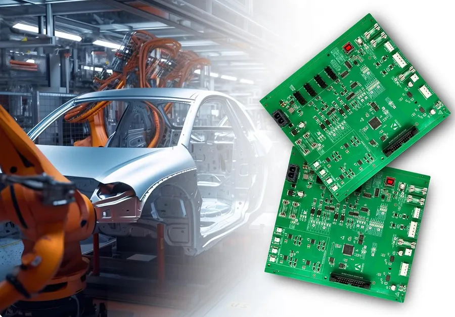
Printed wiring boards (PWBs), whether in their bare form or as populated printed circuit boards (PCBs), are integral components across a multitude of industries. Their versatility stems from their ability to provide a stable platform for electronic components and facilitate electrical connectivity, which makes them indispensable in everything from everyday consumer devices to highly specialized industrial applications. The following sections illustrate the diverse roles PWBs play in various sectors.
Consumer Electronics PWBs are the backbone of consumer electronic devices. Smartphones, tablets, laptops, gaming consoles, and home entertainment systems all rely on PWBs for interconnecting their complex circuitry. The demand for smaller, more powerful, and energy-efficient devices continues to drive advancements in PWB technology within this sector.
Industrial Equipment In industrial settings, PWBs are essential in control systems, automation equipment, robotics, and power supplies. Their robust nature and reliability are paramount in these often demanding environments, and they play a critical role in maintaining consistent and accurate operations.
Automotive Systems Modern vehicles are increasingly reliant on complex electronics systems. From engine management and infotainment to safety systems and advanced driver-assistance systems (ADAS), PWBs are integral to the functionality and reliability of these components. The high operating temperatures and vibration of automotive applications necessitate PWBs constructed from materials capable of withstanding harsh environments.
Medical Devices PWBs are utilized in a wide array of medical devices, including diagnostic equipment, patient monitoring systems, and surgical tools. The precise, consistent operation, high reliability, and compactness of PWBs are crucial in medical applications. Medical devices often require compliance with strict quality and safety regulations.
Aerospace Technologies Aerospace applications demand extreme reliability and high-performance, making PWBs crucial for aircraft control systems, communication devices, satellite equipment and navigation systems. The stringent operational conditions including temperature variation, vibration and radiation exposure necessitate the use of specialized, high-performance PWB materials and designs.
Telecommunications Telecommunications infrastructure relies heavily on PWBs for network switches, routers, base stations and other communication hardware. High signal integrity and reliability are key considerations when designing PWBs for high-speed data transfer.
Frequently Asked Questions About Printed Wiring Boards
This section addresses common inquiries about printed wiring boards (PWBs), offering clear and concise answers to help clarify their role and usage in electronics. This information will help differentiate PWBs from PCBs, while explaining their continued relevance in modern technology.
What exactly is a printed wiring board (PWB)? A printed wiring board (PWB) is a foundational substrate, typically made of insulating material such as fiberglass or composite, upon which electronic components are mounted and interconnected. It provides the physical support and electrical pathways for these components before they are populated. Essentially, it’s the bare board before components are added.
What distinguishes a PWB from a PCB? While the terms are often used interchangeably, technically, a PWB refers to the bare board that provides physical structure and electrical connections. Once electronic components are mounted and soldered onto the PWB, it becomes a Printed Circuit Board (PCB). Thus, a PCB is essentially a populated PWB. However, in modern usage, the terms are often used synonymously.
Is there a difference between a PWA and a PCB? Yes, there is a subtle difference. A PWA, or Printed Wiring Assembly, refers to the complete assembly of the PCB with all components mounted, soldered, and ready for use within an electronic device. A PCB is simply the populated board itself, while the PWA is the functional assembly.
Are printed wiring boards and printed circuit boards still in use? Absolutely. Both printed wiring boards (as a substrate) and printed circuit boards (the populated assembly) are fundamental to modern electronics. They serve as the backbone for nearly all electronic devices, from smartphones and computers to industrial and medical equipment. Their adaptability and versatility mean they remain critical components in current and future technology.
What materials are typically used to make a PWB? Common materials include FR-4 (a fiberglass composite), polyimide (for flexible PWBs), and metal cores (for heat dissipation). Material selection depends on thermal, electrical, and mechanical requirements of the application, including flexibility and operating temperature.
How does PWB design impact the performance of electronic devices? PWB design is crucial for optimal device performance. Factors like trace width and spacing, impedance control, layer stack-up, and routing directly influence signal integrity, electromagnetic compatibility, and overall reliability. A poorly designed PWB can lead to signal loss, noise, and operational failures.
What are some common applications of PWBs? PWBs are ubiquitous, finding applications across all electronic sectors, including consumer electronics, automotive systems, industrial control equipment, aerospace, and medical devices. They are indispensable for connecting components in a vast array of products.
Future Trends in Printed Wiring Board Technology
The printed wiring board (PWB) industry is continually evolving, driven by the relentless pursuit of smaller, faster, and more efficient electronic devices. This section explores the emerging trends that are poised to shape the future of PWB technology, emphasizing advancements in materials, interconnection methods, flexibility, and environmental sustainability.
These trends represent significant advancements in PWB technology, with each addressing specific limitations of existing methods. For example, HDI technologies help enable higher component density and faster signal transmission, flexible PWBs allow for novel product designs, and sustainable manufacturing contributes to eco-friendly production practices. These advancements will not only affect the technological capabilities of electronic devices but also influence how they are designed, manufactured, and integrated into various applications.
Advanced Materials Research into new materials beyond traditional FR-4 is expanding, including high-performance polymers, ceramics, and composites that offer superior thermal management, electrical properties, and mechanical strength. These materials are essential for demanding applications such as high-speed computing, aerospace, and automotive electronics.
High-Density Interconnect (HDI) Technology HDI technology is crucial for achieving higher component density and improved signal integrity. It includes microvias, fine-line traces, and advanced layer stack-ups, allowing more complex circuitry in smaller footprints. These techniques are vital for the miniaturization of devices such as smartphones and wearables.
Flexible and Stretchable PWBs Flexible PWBs, constructed using flexible substrates like polyimide, enable electronic devices to conform to non-planar shapes and withstand mechanical stress. Stretchable PWBs are under development, potentially integrating directly into clothing and biological systems, broadening the scope of electronic applications.
Sustainable Manufacturing Practices The push towards eco-friendly PWB manufacturing is gaining momentum. This includes the use of lead-free materials, water-based processing chemicals, and energy-efficient production techniques. The goal is to minimize the environmental impact of PWB production and meet growing regulatory demands.
Embedded Components and Substrates Embedding components directly within the PWB substrate reduces the need for surface-mounted components, decreasing overall size and improving reliability. This approach also enhances thermal management by integrating heat-generating components more efficiently.
The printed wiring board is an essential component at the heart of modern electronics. Understanding PWBs, their history, their design, their manufacturing, and their future trends, provides valuable insight into the technology that shapes our world. As electronics continue to evolve, PWBs will remain at the core of innovation, adapting to meet the ever-increasing demands of technology and human society.