In the realm of modern electronics, the ubiquitous transistor plays a pivotal role, acting as the fundamental building block for countless devices. Among these, the PNP transistor stands out, a versatile component that controls the flow of electrical current in diverse applications. Much like a water faucet controls water flow in a plumbing system, the PNP transistor precisely manages electrical current, enabling sophisticated control and amplification within electronic circuits. This article explores the inner workings of PNP transistors, providing a deep dive into their characteristics, applications, and differences from their NPN counterparts.
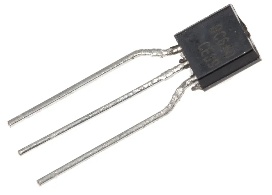
A PNP transistor is a type of bipolar junction transistor (BJT) characterized by its unique layered semiconductor structure: a thin layer of N-type semiconductor material is 'sandwiched' between two layers of P-type semiconductor material. This configuration dictates its operational behavior, fundamentally differing from its NPN counterpart. Crucially, in a PNP transistor, 'holes' serve as the primary charge carriers within the P-type regions, while electrons are the primary charge carriers in the N-type region. This distinction in charge carrier type is key to understanding the transistor's function.
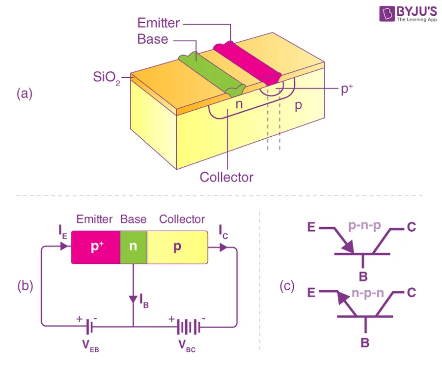
The physical structure of a PNP transistor is characterized by three distinct layers: the emitter, base, and collector. These layers are created through a process of doping semiconductor materials with specific impurities. The PNP transistor is composed of a thin layer of N-type semiconductor material (the base) sandwiched between two layers of P-type semiconductor material (the emitter and collector). The controlled introduction of impurities (dopants) during manufacturing creates these P-N junctions, which are essential for transistor operation.
| Region | Type | Doping Level | Function |
|---|---|---|---|
| Emitter | P-type | Heavily doped | Supplies holes to the base region |
| Base | N-type | Lightly doped | Controls the flow of holes between emitter and collector |
| Collector | P-type | Moderately doped | Collects the holes from the base region |
The doping levels in each region are crucial to the functionality of the transistor. The emitter is heavily doped to provide a large number of charge carriers (holes), while the base is lightly doped to minimize recombination of holes. The collector is moderately doped to efficiently receive holes from the base. The junctions between these layers (emitter-base junction and collector-base junction) create the necessary potential barriers that allow the transistor to operate.
The schematic symbol for a PNP transistor is a circle with three leads representing the emitter, base, and collector. The key distinguishing feature of a PNP transistor's symbol is the arrow on the emitter lead pointing towards the base. This arrow indicates the direction of conventional current flow (positive charge) when the transistor is active. This is in contrast to NPN transistors where the arrow points outwards.
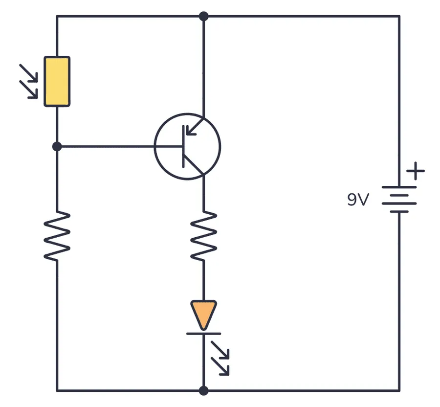
The operation of a PNP transistor hinges on the manipulation of current flow through its three terminals: the emitter, the base, and the collector. Unlike its NPN counterpart, a PNP transistor activates when the base voltage is pulled *lower* than the emitter voltage, a condition that facilitates the movement of charge carriers and allows current to flow from the emitter to the collector.
At its core, the PNP transistor is constructed with a thin layer of N-type semiconductor material (the base) sandwiched between two layers of P-type material (the emitter and collector). In a typical configuration, the emitter is connected to a positive voltage, the collector is connected to a load (such as a resistor), and the base is connected to a control circuit. When the base voltage is sufficiently negative compared to the emitter, it forward biases the base-emitter junction, leading to a flow of holes (the primary charge carriers in P-type material) from the emitter into the base. This injection of holes into the base region reduces the potential barrier between the base and collector, enabling a larger current of holes to flow from the emitter, through the base, and into the collector.
Imagine a valve controlling the flow of water; the base of a PNP transistor acts in a similar manner. When the base voltage is close to or greater than the emitter voltage, the "valve" is closed, and only a very small leakage current can flow. However, when the base voltage is reduced significantly below the emitter voltage, the "valve" opens, allowing a large current to flow from the emitter to the collector. Crucially, a small change in base voltage can create a significant change in the collector current, demonstrating the transistor's ability to act as a current amplifier or switch.
In summary, a PNP transistor's operation relies on the forward biasing of the base-emitter junction by pulling the base voltage lower than the emitter voltage. This action allows a large current to flow from the emitter to the collector. This characteristic is what allows it to be used effectively as a switch or an amplifier.
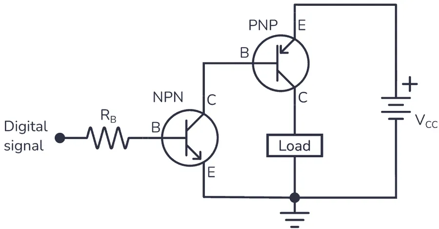
The PNP transistor functions effectively as an electronic switch, controlling current flow in a circuit. Unlike mechanical switches, transistors provide fast, reliable switching without physical contacts, making them essential in modern electronics. The key to using a PNP transistor as a switch lies in manipulating the base current to control the larger current flow between the emitter and collector.
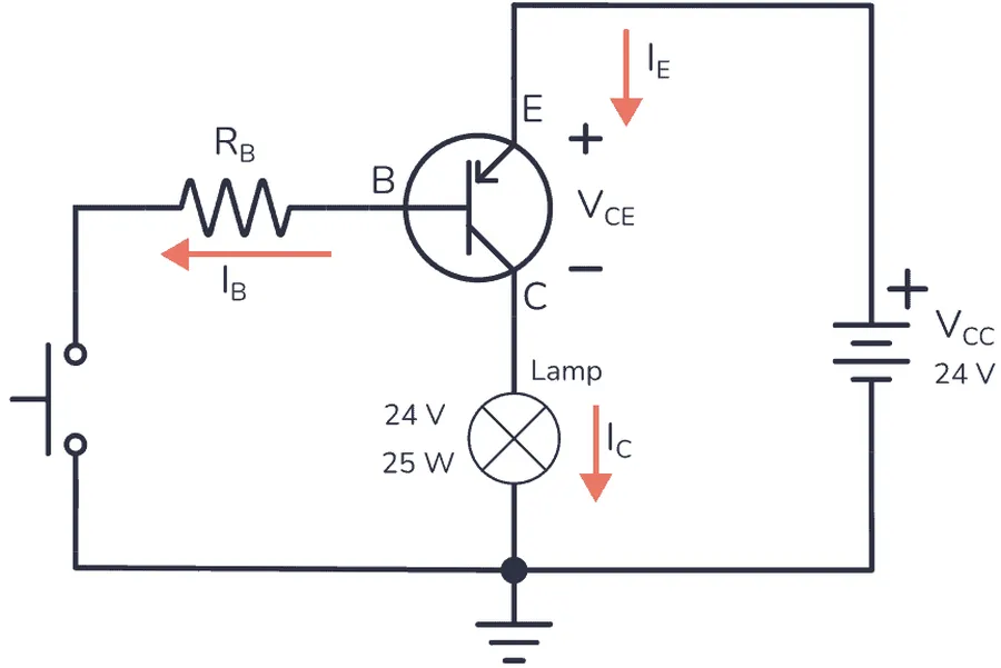
A PNP transistor acts as a 'high-side' switch, meaning it's typically placed between a power source and the load. In this configuration, the transistor is 'on' when no current flows into its base, allowing current to flow from emitter to collector. When a current is applied to the base terminal, the transistor switches 'off', blocking the current flow. This makes PNP transistors ideal for applications requiring a device to be switched on by default.
Consider a practical scenario: controlling a small motor using a microcontroller. The microcontroller's output pin might be too weak to directly power the motor. A PNP transistor can act as an intermediary. When the microcontroller outputs a low signal, this triggers a current flow through the base of the PNP transistor and shuts off the transistor, turning off the motor. Conversely, when the microcontroller output is high, no current flows into the base of the transistor, the transistor turns on and powers the motor. This enables the microcontroller to control a higher current, higher voltage device with its relatively low-power output signal.
The voltage requirements for switching a PNP transistor typically involve ensuring the base-emitter junction is forward-biased to either allow or block current flow. For instance, in a circuit with a 5V power supply, the base would typically need to be a little lower than the emitter voltage to turn the transistor on. Conversely, when the base is at, or higher than, the emitter voltage, the transistor turns off. Similarly, current requirements vary depending on the transistor's type and load. A small base current can control a much larger emitter-collector current, but the specific amounts depend on the transistor's current gain, hFE parameter, and its respective datasheet.
Below is a simplified representation of a PNP transistor switch circuit, depicting how a load can be controlled by adjusting the voltage applied to the transistor's base:
PNP transistors, beyond their switching capabilities, exhibit a powerful ability to amplify electrical signals. This amplification arises from the transistor's inherent characteristic of controlling a larger collector current with a smaller base current, effectively boosting the signal's magnitude.
The underlying principle of PNP transistor amplification relies on the modulation of current flow between the collector and emitter by a much smaller current applied to the base. Specifically, a slight change in base current causes a significant change in collector current. This functionality makes the PNP transistor invaluable in signal processing applications where amplification of a weak signal is paramount.
A common amplifier configuration using a PNP transistor is the common-emitter amplifier. In this setup, the emitter is common to both the input and output circuits. The input signal is applied to the base, and the amplified output signal is taken from the collector. This configuration allows for voltage gain, meaning the output signal is a larger version of the input signal. Proper biasing is crucial to establish the correct operating point for linear amplification without signal distortion.
The circuit biasing for a PNP transistor based amplifier will be different than for an NPN transistor based amplifier. For the PNP configuration the base is biased more negatively than the emitter, this allows a small base current to cause a larger current to flow between the collector and the emitter. The amplifier is designed so that the applied input signal varies the base current around the bias point.
Consider the following simplified explanation of how the common-emitter amplifier works. A small change in the base current of the PNP transistor results in a relatively large change in the collector current. The current gain is approximately equal to the ratio of collector current to the base current (β). The voltage gain is dependent on other circuit elements but will be proportional to the current gain. The voltage gain is the ratio of the output signal to the input signal.
When utilizing a PNP transistor as an amplifier, care should be taken to manage the associated heat production, selecting an appropriate transistor to suit the requirements of the circuit. Choosing components correctly can guarantee the operational efficiency and longevity of the amplifier circuit.
// Basic common-emitter amplifier circuit using a PNP transistor
//  Note: This is a simplified illustrative circuit, actual
//  implementations may require additional components.

/*
*   VCC ----+--- Rc ---+--- Collector
*           |            |
*           |           PNP
*           |           Transistor
*           |            |
*  Input ---+--- Rb ---+--- Base
*                     |
*           |         Emitter
*           +---------GND
*   VCC = Voltage Common Collector
*   Rc = Collector Resistor
*   Rb = Base Resistor
*   Input = Signal input
*/
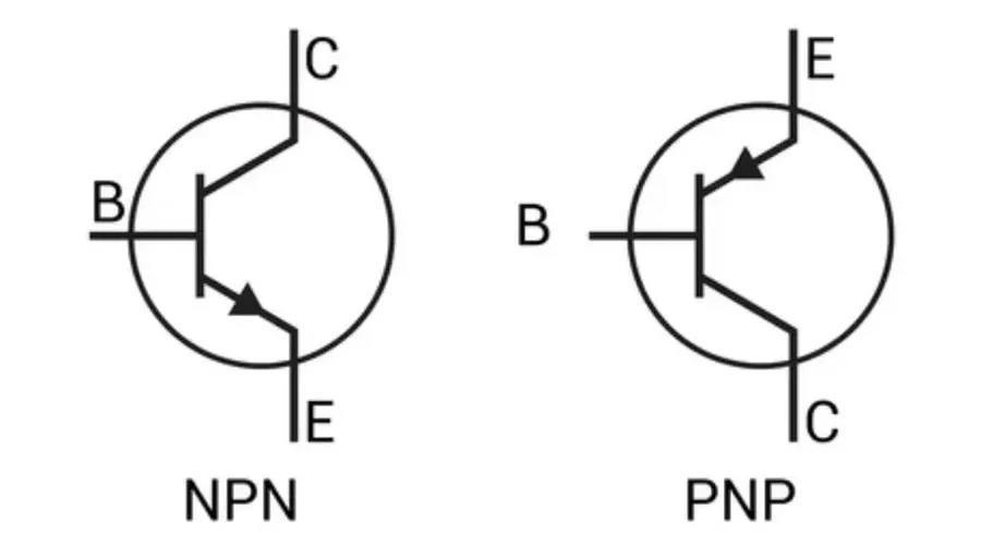
NPN and PNP transistors are fundamental bipolar junction transistors (BJTs), each with distinct characteristics that determine their application in electronic circuits. The primary difference lies in their doping profiles, resulting in opposite voltage polarities for activation and reversed current flow directions.
| Feature | NPN Transistor | PNP Transistor |
|---|---|---|
| Doping Profile | N-P-N (N-type emitter, P-type base, N-type collector) | P-N-P (P-type emitter, N-type base, P-type collector) |
| Activation Voltage | Positive base-emitter voltage (Vbe > 0.7V typically) | Negative base-emitter voltage (Vbe < -0.7V typically) |
| Current Flow Direction | Conventional current flows from collector to emitter | Conventional current flows from emitter to collector |
| Bias Requirement | Base needs to be more positive than the emitter | Base needs to be more negative than the emitter |
| Typical Use Cases | Low-side switching, current sinking | High-side switching, current sourcing |
| Charge Carriers | Electrons | Holes |
Understanding these key differences is essential for selecting the correct transistor for a specific application. NPN transistors are often chosen for low-side switching, where the load is connected between the transistor's collector and the positive supply rail. PNP transistors are typically employed for high-side switching, where the load is connected between the transistor's emitter and ground. The choice is primarily dictated by how the circuit needs to interface with power and ground potentials.
PNP transistors, characterized by their unique current flow and activation requirements, find extensive use in various electronic applications. They are particularly well-suited for scenarios where high-side switching, current sourcing, or push-pull configurations are needed, often offering advantages over their NPN counterparts in these specific roles.
The choice between PNP and NPN transistors for a specific application hinges on the polarities of the circuit and the desired current flow direction. While NPN transistors are commonly used for low-side switching (connecting the load to ground) and current sinking, PNP transistors are advantageous when high-side switching or current sourcing is required. For example, in situations where a device needs to be powered directly by a high voltage source, and that source needs to be switched, a PNP would be required over an NPN.
Below are examples where PNP transistors are favored, along with diagrams illustrating their usage.
This section addresses common queries about PNP transistors, providing clear and concise answers to help solidify your understanding of these essential electronic components. We aim to clarify key concepts, operational principles, and practical aspects of using PNP transistors.
When integrating PNP transistors into circuit designs, several practical factors demand careful attention to ensure optimal performance and reliability. These include selecting the correct transistor for the application, managing power dissipation to prevent damage, and implementing appropriate biasing techniques for stable operation. Furthermore, understanding common troubleshooting steps and identifying various package types are crucial skills for any electronics engineer or hobbyist.
In conclusion, the PNP transistor is a fundamental building block of modern electronics. Its ability to control current flow and amplify signals makes it indispensable in a wide array of applications. Understanding its working principles, construction, and differences from its NPN counterpart is crucial for any aspiring electronics engineer. From simple switching circuits to complex audio amplifiers, the PNP transistor continues to play a vital role in innovation, highlighting its lasting significance in the world of electronic design. As technology progresses, the versatility and importance of the PNP transistor remains steadfast, underscoring its pivotal place in the field of electronics.

