The Bipolar Junction Transistor (BJT), a cornerstone of modern electronics, acts as a versatile switch and amplifier in countless devices, from simple radios to complex computer systems. Like the human nervous system which uses electrical signals to function, BJT transistor amplifies or switches electrical current. This article explores their structure, types, working principles, and diverse applications in electronics, providing clear and actionable insights.
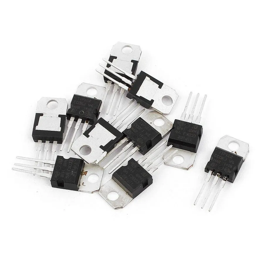
A Bipolar Junction Transistor (BJT) is a three-terminal semiconductor device fundamentally operating as a current-controlled current source. It is a cornerstone component in electronics, serving primarily as an amplifier or a switch. The BJT's operation hinges on the manipulation of current flow between its terminals by altering the current at its control terminal, demonstrating a clear principle of current amplification and control.
Key to understanding the BJT are its three terminals: the emitter, base, and collector. These terminals are formed through a sandwiching of semiconductor materials, where either a P-type material is layered between two N-type materials (NPN transistor) or an N-type material is layered between two P-type materials (PNP transistor). The doping of these regions determines the behavior and type of transistor, a critical design parameter to control the charge carrier flow and overall electrical properties of the device.
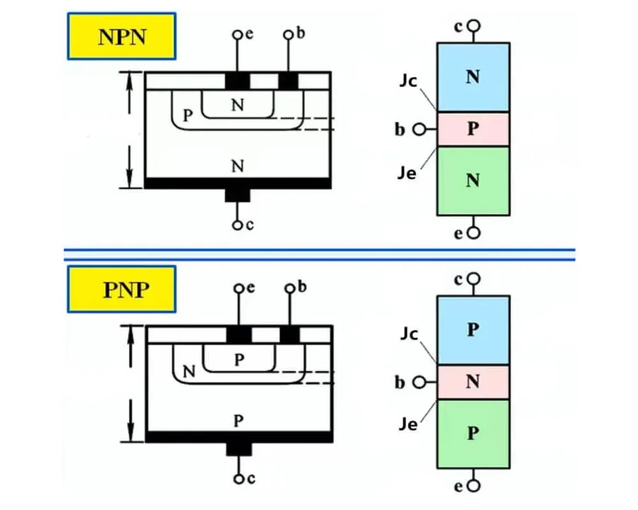
Bipolar Junction Transistors (BJTs) are three-terminal semiconductor devices constructed from a precisely layered arrangement of P-type and N-type materials. These layers create two PN junctions that dictate the transistor's behavior. The two primary configurations are NPN and PNP, distinguished by the sequence and doping of their layers.
The core of a BJT consists of three distinct regions: the emitter, the base, and the collector. The emitter serves as the source of charge carriers, while the collector gathers these carriers. The base, a very thin middle region, controls the flow of charge carriers between the emitter and the collector. The way these layers are arranged, and their specific doping levels, dictate whether the device operates as an NPN or PNP transistor.
| Feature | NPN Transistor | PNP Transistor |
|---|---|---|
| Layer Arrangement (from emitter to collector) | N-P-N | P-N-P |
| Majority Carriers | Electrons | Holes |
| Doping Levels | Emitter: Heavily doped, Base: Lightly doped, Collector: Moderately doped | Emitter: Heavily doped, Base: Lightly doped, Collector: Moderately doped |
| Current Flow (Conventional) | From collector to emitter when active | From emitter to collector when active |
The precise control over doping concentrations and layer thicknesses is vital for achieving desired electrical characteristics in BJTs. For instance, the base region is intentionally made very thin and lightly doped compared to the emitter and collector. This thin base allows for efficient current amplification, as most charge carriers from the emitter successfully cross the base and reach the collector. Additionally, the doping levels in the emitter are generally higher than those of the collector, optimizing current injection. The collector region is designed to handle the bulk of the current and is moderately doped.
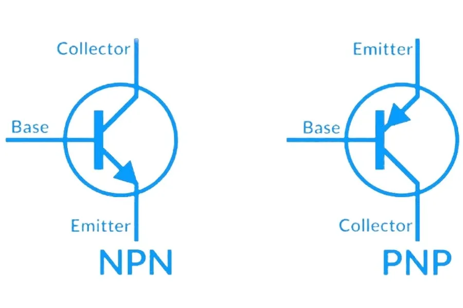
Bipolar junction transistors (BJTs) come in two primary configurations: NPN and PNP. These configurations differ in their semiconductor material arrangement and the resulting direction of current flow, influencing their application in electronic circuits. Understanding the distinctions between NPN and PNP transistors is fundamental for effective circuit design.
| Feature | NPN Transistor | PNP Transistor |
|---|---|---|
| Structure | N-type emitter, P-type base, N-type collector | P-type emitter, N-type base, P-type collector |
| Current Flow (Conventional) | Collector to Emitter | Emitter to Collector |
| Polarity for Active Region | Base-Emitter junction forward biased (VBE > 0), Collector-Base junction reverse biased (VCB > 0) | Base-Emitter junction forward biased (VEB > 0), Collector-Base junction reverse biased (VBC > 0) |
| Base Current Direction (Conventional) | Into Base | Out of Base |
| Majority Charge Carriers | Electrons in the emitter and collector, Holes in the base | Holes in the emitter and collector, Electrons in the base |
| Typical Application Areas | Lower-side switching, logic circuits, general amplification | High-side switching, power circuits, specific amplifier configurations |
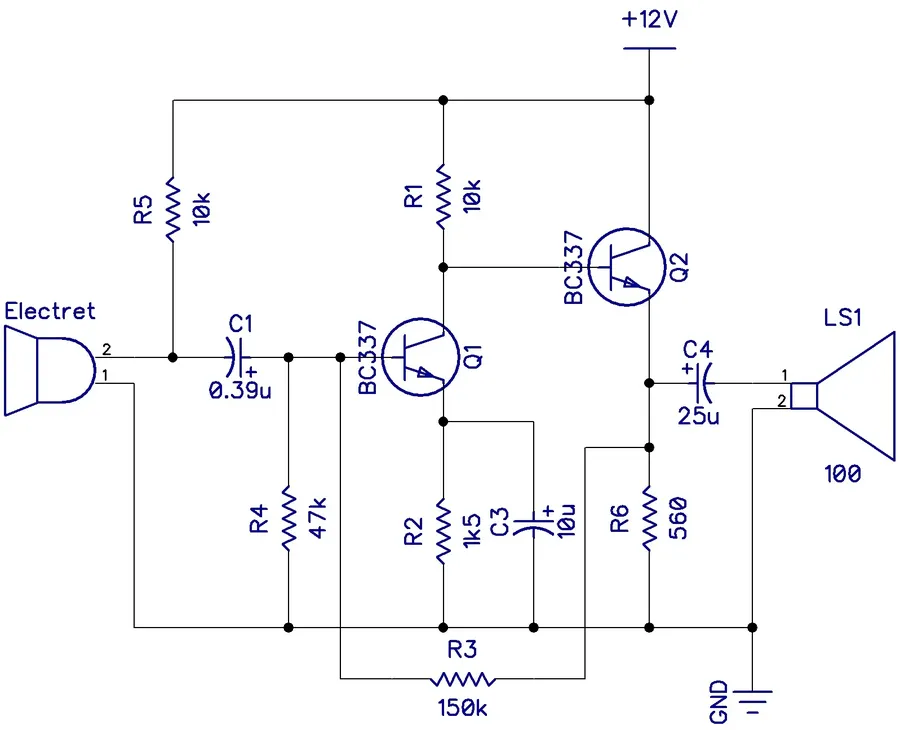
The Bipolar Junction Transistor (BJT) functions fundamentally as a current-controlled current source. This means that a small current applied to the base terminal modulates a larger current flowing between the collector and emitter terminals. This core characteristic enables the BJT to perform two essential functions: amplification and switching. The underlying mechanism is rooted in the manipulation of charge carrier flow within the semiconductor materials.
In amplification, a small time-varying signal applied to the base modulates the collector current, producing a larger but proportional signal at the output. When used as a switch, the base current acts as the control signal, either allowing or preventing current flow between the collector and emitter, thereby enabling the BJT to function as an electronic on/off switch.
| Aspect | Amplification | Switching |
|---|---|---|
| Function | Increase signal strength | Control current flow |
| Operation | Proportional modulation of collector current by base current | Base current acts as a gate for collector current |
| Application | Audio amplifiers, signal processing | Digital logic, power control |
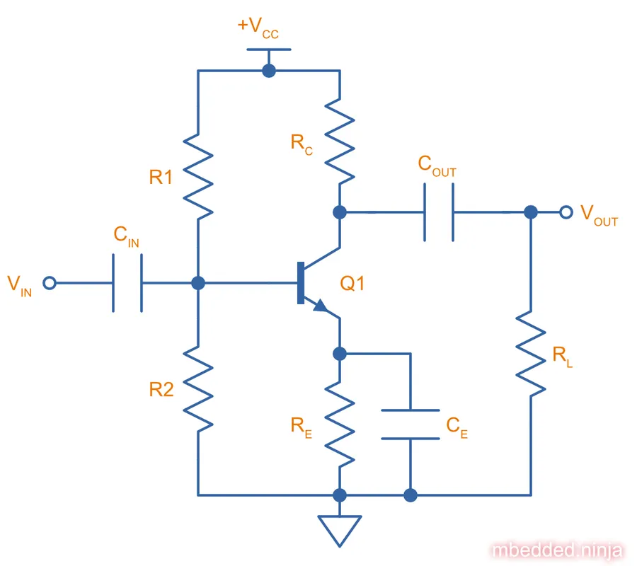
Bipolar Junction Transistors (BJTs) are versatile devices, and their functionality in circuits is significantly influenced by the configuration in which they are connected. There are three fundamental BJT configurations: common emitter (CE), common base (CB), and common collector (CC), each exhibiting distinct input/output characteristics, gains, and impedance, making them suitable for specific applications.
| Configuration | Input Terminal | Output Terminal | Voltage Gain | Current Gain | Input Impedance | Output Impedance | Typical Uses |
|---|---|---|---|---|---|---|---|
| Common Emitter (CE) | Base | Collector | Medium to High | High | Medium | Medium | Voltage amplification, general-purpose amplifiers |
| Common Base (CB) | Emitter | Collector | High | Close to 1 | Low | High | High-frequency applications, impedance matching |
| Common Collector (CC) | Base | Emitter | Close to 1 | High | High | Low | Current amplification, impedance buffering |
Understanding the key parameters of a BJT transistor is crucial for effective circuit design and analysis. These parameters dictate how the transistor will behave in a circuit, influencing its amplification, switching speed, and overall performance. The primary parameters include current gain (β and α), transconductance (gm), and breakdown voltage (VBR), each playing a vital role in different applications.
| Parameter | Symbol | Definition | Typical Value Range | Impact on Circuit | Application Relevance |
|---|---|---|---|---|---|
| DC Current Gain (Beta) | β (hFE) | Ratio of collector current (IC) to base current (IB) in DC operation. | 20 to 500 | Determines the transistor's current amplification capability. Higher β implies a larger collector current for a given base current. | Amplifier circuits, where high current gain is desired. |
| Common-Base DC Current Gain (Alpha) | α (hFB) | Ratio of collector current (IC) to emitter current (IE) in DC operation. | 0.95 to 0.99 | Indicates the fraction of emitter current that reaches the collector. Close to unity. | Used less frequently in practical applications, but important for theoretical analysis of BJT operation. |
| Transconductance | gm | Ratio of change in collector current (ΔIC) to change in base-emitter voltage (ΔVBE). | Typically a few millisiemens to several siemens. | Measures how effectively a change in input voltage controls the output current, essential for amplifiers | Amplifier circuits, especially for small-signal analysis. |
| Breakdown Voltage | VBR | The reverse voltage at which the transistor starts conducting excessively, possibly damaging it. | Tens to hundreds of volts, depending on the specific BJT. | Limits the maximum usable voltage across the transistor, preventing damage from overvoltage. Must always be considered during design. | Power switching and high-voltage applications. |
| Saturation Voltage | VCE(sat) | The voltage drop across the collector and emitter when the transistor is in saturation mode. | Usually very low, a few hundred millivolts. | Affects the switching efficiency of the transistor, lower voltage indicates less power dissipation. | Switching applications, as it determines the 'on' state voltage. |
| Cutoff Current | ICEO | The collector current when the base current is zero. This is a leakage current. | Typically in the nanoampere to microampere range. | Represents leakage current, can affect temperature stability. | Critical in high-temperature environments. |
Choosing the right transistor depends on the specific needs of the application. For instance, a high-β transistor is ideal for applications requiring significant current amplification, while a transistor with a high breakdown voltage is necessary for high-voltage applications. Transconductance is essential when designing amplifier circuits, as it determines the voltage gain.
This section addresses common questions regarding BJT transistors, providing clear and concise answers to enhance understanding of their functionality and applications. These questions are crucial for both beginners and experienced users to effectively utilize BJT transistors in electronic circuit designs.
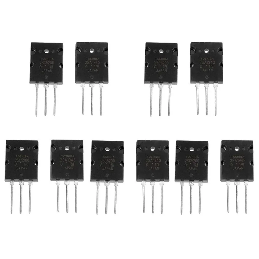
Bipolar Junction Transistors (BJTs), despite the rise of MOSFETs, remain crucial components in numerous electronic applications due to their unique characteristics. Their ability to provide current amplification and operate as switches makes them suitable for both analog and digital circuits. Below, we explore specific applications where BJT transistors excel.
Bipolar Junction Transistors (BJTs), while fundamental in electronics, present a mix of advantages and disadvantages when compared to other transistor types such as MOSFETs. Understanding these trade-offs is crucial for making informed design choices. This section provides a detailed comparison, including example use cases to illustrate each point.
| Feature | BJT Transistors | MOSFET Transistors |
|---|---|---|
| Input Impedance | Low | High |
| Current Gain | High | Moderate |
| Voltage Gain | Moderate | High |
| Switching Speed | Moderate | High |
| Power Consumption | Higher (due to base current) | Lower |
| Temperature Sensitivity | More Sensitive | Less Sensitive |
| Cost | Generally Lower | Generally Higher |
| Complexity | Relatively Complex for biasing | Simpler |
| Typical Applications | Amplifiers, Analog circuits, Switching | Digital Logic, High-Speed Switching, Power Management |
The advantages of BJTs include their high current gain, making them suitable for applications requiring significant current amplification. Additionally, BJTs are often more economical than MOSFETs, which can be a significant factor in cost-sensitive designs. However, BJTs require a base current to operate, leading to higher power consumption compared to MOSFETs, which are voltage-controlled devices. The lower input impedance of BJTs can also pose a challenge in some circuit designs where a higher impedance is needed. Additionally, they exhibit higher temperature sensitivity, which can affect their performance under varying conditions.
For example, in audio amplifiers, the high current gain of BJTs allows them to drive speakers effectively, but their temperature sensitivity might require careful biasing to avoid thermal runaway. On the other hand, MOSFETs with their high input impedance and low power consumption are preferred in digital logic circuits where signal integrity and efficiency are crucial. In switching power supplies, the lower power consumption of MOSFETS and ability to operate at higher switching speeds make them a superior choice.
In summary, while BJTs remain a valuable component in many electronic circuits, a thorough understanding of their advantages and disadvantages, and their characteristics in comparison to other types of transistors such as MOSFETs, is necessary when designing a new application.
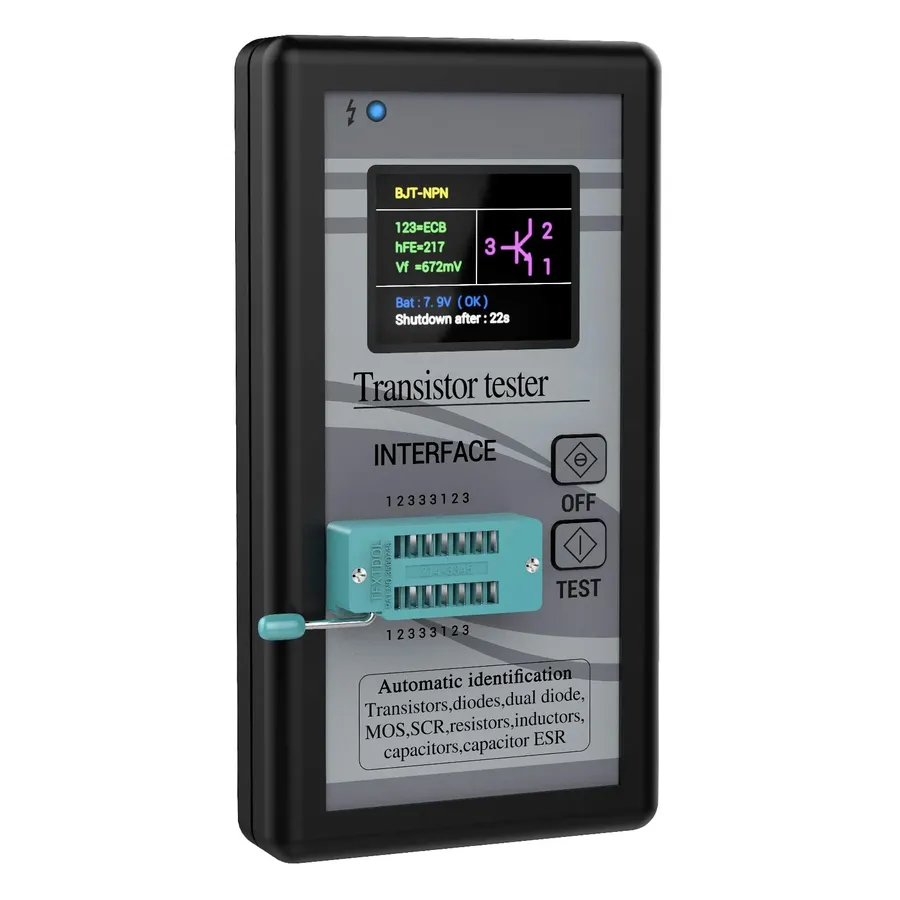
Selecting the appropriate BJT transistor for a specific circuit design and verifying its functionality are critical steps in electronic engineering. This process ensures that the transistor meets the circuit's performance requirements and operates reliably within specified parameters. Proper selection and testing are essential for successful circuit operation and avoiding potential failures.
Once the appropriate BJT transistor has been selected, it's essential to verify its basic functionality before incorporating it into a complex circuit. Simple tests can be performed using a multimeter to confirm that the transistor is operating correctly.
Bipolar Junction Transistors (BJTs), though not always the star of the show in today's highly digital world, remain foundational devices in countless electronics. From fundamental signal amplification to power management circuits, BJT transistors are a testament to the ingenious use of semiconductor materials. A firm grasp of BJT structure, functionality, and usage remains crucial for both aspiring and experienced electronic enthusiasts and engineers alike, ensuring its continued relevance in future technologies.

