In an era where personal well-being is paramount, wearable technology has emerged as a transformative force, bringing health monitoring directly to our wrists. At the heart of every sophisticated health-tracking device lies a marvel of miniaturization and precision engineering: the Printed Circuit Board (PCB). As a veteran engineer from Zero One Solution Limited, I understand the critical role these tiny, yet powerful, components play in bringing your innovative wearable health monitoring bracelet concepts to life. This article will delve into the intricacies of designing and manufacturing robust PCB solutions tailored specifically for the dynamic demands of wearable health devices, highlighting how Zero One Solution Limited empowers you to accelerate product development and achieve market success.
The Evolution of Wearable Health Technology and PCB's Role
The rapid ascent of wearable health technology has transformed personal healthcare, shifting from reactive treatment to proactive monitoring. At the heart of this revolution is the Printed Circuit Board (PCB), serving as the indispensable central nervous system for devices like health monitoring bracelets. These compact, intelligent systems enable sophisticated real-time data collection and analysis directly from the wrist, fundamentally changing how individuals engage with their health. The demand for increasingly miniaturized, power-efficient, and supremely reliable PCB solutions in this burgeoning market is paramount, driving continuous innovation in design and manufacturing.
Early Wearables (2000s-Early 2010s) Initial wearable devices were primarily pedometers and basic fitness trackers. PCBs were relatively simple, focusing on core functionality like step counting and calorie estimation. Size and power consumption were concerns, but not yet critical drivers as devices were larger and battery life expectations were lower.
Smartwatch Era (Mid-2010s) The advent of smartwatches expanded wearable capabilities to include heart rate monitoring, GPS, and notifications. This necessitated more complex, multi-layered PCBs to accommodate a wider array of sensors and communication modules. Miniaturization became a significant challenge, pushing PCB manufacturers to refine their processes for denser component integration.
Advanced Health Monitoring (Late 2010s-Present) Today's health monitoring bracelets integrate medical-grade sensors for ECG, SpO2, continuous body temperature, and more. This requires highly sophisticated, often rigid-flex PCBs to balance advanced sensor integration with ergonomic designs. Signal integrity, power efficiency for always-on monitoring, and robust environmental resistance are critical, making the PCB a highly specialized and complex component.
PCB Attribute
Early Wearables (2000s)
Modern Health Bracelets (2020s)
Complexity
Low (Single/Double Layer)
High (Multi-Layer, Rigid-Flex)
Component Density
Low
Very High
Power Consumption
Moderate
Ultra-Low (Critical)
Sensor Integration
Basic (Accelerometer)
Advanced (ECG, PPG, SpO2, Temp)
Form Factor
Larger, less conformal
Miniaturized, highly ergonomic
Data Handling
Basic tracking
Real-time, complex analytics
Key Challenges in Wearable Health Monitoring Bracelet PCB Design
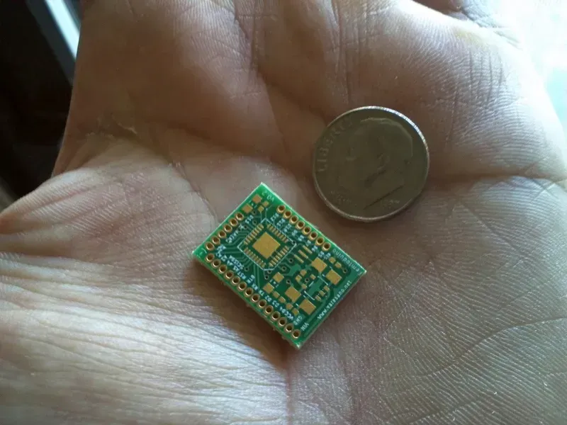
Miniature PCB Board Design
Designing Printed Circuit Boards (PCBs) for wearable health monitoring bracelets presents a unique confluence of engineering hurdles that demand specialized expertise. Unlike conventional electronics, wearables operate in close proximity to the human body, enduring constant movement, varying temperatures, and often, moisture. This necessitates a PCB that is not only compact and powerful but also exceptionally robust and reliable. Overcoming these challenges is paramount to delivering accurate, continuous, and user-friendly health monitoring devices that meet stringent performance and safety standards.
Why is miniaturization critical for wearable health monitoring bracelet PCBs? Miniaturization is crucial because wearable devices, particularly health monitoring bracelets, must be small, lightweight, and unobtrusive to ensure user comfort and compliance. This demands highly integrated components, advanced packaging technologies, and multi-layer PCB designs to fit complex functionalities into minimal space without compromising performance or thermal management.
How does Zero One Solution Limited ensure power efficiency in wearable health monitoring bracelet PCB designs? Zero One Solution Limited optimizes power efficiency through careful component selection, prioritizing low-power microcontrollers and specialized power management ICs. We implement intelligent power routing, impedance control, and advanced design techniques to minimize current leakage and maximize battery life, which is critical for continuous health monitoring.
What are the primary signal integrity challenges for biosensors on wearable PCBs? Biosensors generate very low-level analog signals that are highly susceptible to noise and interference. Key signal integrity challenges include minimizing electromagnetic interference (EMI) from digital circuits, ensuring stable power delivery to sensitive analog components, and precise routing of signal traces to prevent crosstalk and maintain signal fidelity for accurate data acquisition.
How does EMI/EMC compliance impact wearable health monitoring bracelet PCB design? EMI/EMC compliance is vital for wearable PCBs to ensure the device operates reliably without interfering with other electronics or causing self-interference. Design considerations include proper grounding techniques, shielding, strategic component placement to minimize loop areas, and careful selection of materials with appropriate dielectric properties, all to meet international regulatory standards like FCC and CE.
Why are flexible or rigid-flex PCB structures preferred for wearable health monitoring bracelets? Flexible and rigid-flex PCB structures are preferred due to their inherent ability to conform to irregular shapes, withstand repetitive bending and torsion, and reduce the overall device size and weight. This allows for ergonomic designs that better fit the human body, integrate seamlessly with the product's aesthetics, and offer enhanced durability against physical stresses common in wearables.
Essential Components and Technologies for Health Monitoring Bracelets
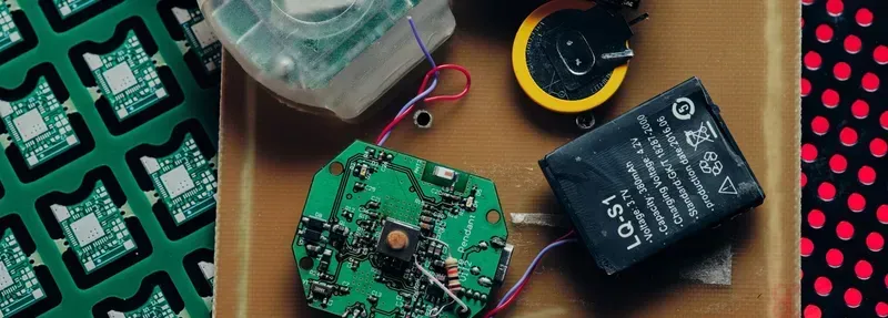
Wearable Health Bracelet Internal Components
The efficacy and intelligence of a wearable health monitoring bracelet are fundamentally determined by the synergistic integration of its essential components on a precisely engineered Printed Circuit Board (PCB). These components, acting as the device's sensory and processing backbone, transform raw physiological data into actionable health insights. The intricate design and seamless integration of these technologies on the PCB are paramount for the bracelet's ability to accurately monitor, analyze, and transmit vital health metrics, truly bringing sophisticated medical-grade monitoring to the user's wrist. Zero One Solution Limited excels in orchestrating this complex interplay, ensuring optimal performance for wearable health monitoring bracelet PCB solutions.
Component Category
Specific Components
Function in Wearable Health Monitoring
PCB Integration Considerations
Biosensors
PPG (Photoplethysmography) Sensors, ECG (Electrocardiogram) Electrodes, Temperature Sensors, Accelerometers/Gyroscopes
Measure heart rate, blood oxygen saturation, electrical activity of the heart, skin temperature, and physical activity/sleep patterns.
Requires careful placement to minimize noise, ensure skin contact, and integrate flexible circuitry for anatomical conformity. Analog front-end (AFE) integration is critical for signal conditioning.
Processing & Control
Microcontrollers (MCUs), Digital Signal Processors (DSPs)
Process raw sensor data, run algorithms for health metrics, manage device functions, and control user interface.
Compact footprints, low power consumption, efficient heat dissipation, and robust power delivery networks are essential due to limited space and battery life.
Wireless Communication
Bluetooth Low Energy (BLE) Modules, NFC (Near Field Communication) Chips
Enable data transfer to smartphones or cloud platforms, facilitate device pairing, and support contactless interactions.
Optimized antenna design and placement to ensure reliable connectivity without interfering with other sensitive components or being impacted by body absorption.
Power Management
Power Management ICs (PMICs), Battery Chargers, Voltage Regulators
Efficiently manage power consumption, charge batteries, and provide stable voltage rails to various components, maximizing battery life.
Requires careful layout for thermal management, minimal electromagnetic interference (EMI), and efficient energy conversion to extend operational time.
Memory
Flash Memory, RAM (SRAM/DRAM)
Store operating system, sensor data logs, user profiles, and application code.
Selection based on required storage capacity and speed, integration into compact packages (e.g., PoP - Package on Package) to save PCB space.
How does miniaturization impact wearable health monitoring bracelet PCB design? Miniaturization is critical for wearable health monitoring bracelet PCB design because it directly impacts device comfort, aesthetics, and user acceptance. Smaller PCBs allow for sleeker, less obtrusive designs, which are essential for products worn continuously. This drives the adoption of advanced packaging technologies like System-in-Package (SiP), Package-on-Package (PoP), and High-Density Interconnect (HDI) PCBs, which allow more components to be integrated into a smaller area while maintaining electrical performance and thermal management. Zero One Solution Limited leverages these advanced techniques to achieve ultra-compact and highly functional PCB layouts for our clients.
Why are biosensors so crucial for health monitoring bracelets? Biosensors are the fundamental data acquisition units in health monitoring bracelets. They directly interact with the user's body to measure physiological parameters such as heart rate (via PPG), electrical activity of the heart (ECG), body temperature, and movement (accelerometer/gyroscope). Without accurate and reliable biosensors, the bracelet cannot collect the raw data necessary for calculating health metrics or detecting anomalies. Their precision and stability are paramount for the device's diagnostic and monitoring capabilities, directly influencing the trustworthiness of the health insights provided to the user.
What role do microcontrollers play in wearable health monitoring bracelet PCBs? Microcontrollers (MCUs) serve as the central processing unit (CPU) on a wearable health monitoring bracelet PCB. They are responsible for collecting raw data from various biosensors, executing complex algorithms to process this data into meaningful health metrics (e.g., heart rate variability, sleep stages), managing communication protocols (like Bluetooth Low Energy), and controlling the device's overall operation and user interface. The choice of MCU is critical for balancing processing power, energy efficiency, and cost, ensuring the bracelet can perform its functions reliably within strict power budgets.
How does Zero One Solution ensure seamless integration of diverse components on a wearable PCB? Zero One Solution Limited ensures seamless integration of diverse components on wearable PCBs through a meticulous design process that emphasizes co-design and comprehensive system-level planning. This includes optimizing component placement to minimize signal interference and electromagnetic compatibility (EMC) issues, designing efficient power delivery networks to support various ICs, and implementing advanced routing strategies for high-speed signals. We utilize sophisticated CAD tools for detailed layout and simulation, followed by rigorous prototyping and testing. Our expertise in rigid-flex and HDI technologies further allows for compact and robust integration, addressing the specific challenges of miniaturization and complex interconnections required for wearable health monitoring bracelet PCBs.
Why is power management critical for wearable health monitoring bracelet PCB solutions? Power management is critical for wearable health monitoring bracelet PCB solutions because these devices are battery-powered and demand extended operational times between charges. Effective power management involves selecting low-power components, designing efficient power management ICs (PMICs) to regulate voltage and current, implementing intelligent power cycling strategies, and optimizing standby modes. Poor power management leads to short battery life, frequent recharging, and a poor user experience. Zero One Solution Limited prioritizes ultra-low power design principles in our PCB solutions, maximizing battery efficiency and ensuring long-term usability for wearable devices.
Zero One Solution's Comprehensive PCB Solutions for Wearables
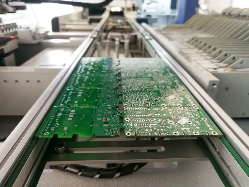
PCB Manufacturing Factory Production Line
At the forefront of innovation, Zero One Solution Limited offers a comprehensive, end-to-end PCB solution specifically engineered for wearable health monitoring bracelets, addressing the unique challenges of miniaturization, power efficiency, and robust performance. Our integrated approach, spanning from initial design to rapid prototyping, precise manufacturing, and efficient assembly, significantly streamlines the development lifecycle, enabling our clients to accelerate time-to-market for their groundbreaking wearable health products with unparalleled quality and reliability. We are the strategic partner that transforms complex concepts into tangible, high-performance wearable devices, cementing our position as a leader in Wearable Health Monitoring Bracelet PCB Solutions.
End-to-End Service Portfolio for Wearable Health Monitoring Bracelet PCB Solutions Zero One Solution Limited provides a seamless, integrated suite of services covering every stage of the PCB development and production for wearable health monitoring bracelets. This includes expert PCB design and layout, leveraging advanced DFM/DFA principles for optimal performance and manufacturability; rapid prototyping services to validate designs quickly; high-precision PCB manufacturing with a focus on tight tolerances and specialized materials; and efficient PCBA services, incorporating advanced SMT and through-hole assembly techniques. This holistic approach minimizes vendor management, reduces lead times, and ensures consistent quality across the entire product lifecycle.
Accelerated Time-to-Market through Rapid Prototyping and Agile Manufacturing Understanding the fast-paced nature of the wearable technology market, Zero One Solution Limited prioritizes rapid prototyping and agile manufacturing processes. Our state-of-the-art facilities and experienced engineering teams enable quick turnaround times for prototype fabrication and iteration, allowing clients to test and refine their wearable health monitoring bracelet designs efficiently. This agility, combined with our streamlined supply chain, is crucial for gaining a competitive edge by bringing innovative products to market faster and more cost-effectively.
Uncompromised Quality and Reliability in Wearable PCB Manufacturing The reliability of wearable health monitoring bracelets is paramount, given their direct interaction with users and critical health data. Zero One Solution Limited adheres to stringent quality control protocols and industry standards (e.g., IPC) throughout the entire manufacturing process. We meticulously select high-grade materials, employ advanced inspection techniques, and conduct rigorous testing, including functional, environmental, and reliability tests, to ensure that every Wearable Health Monitoring Bracelet PCB Solution delivered meets the highest benchmarks for durability, performance, and long-term stability in diverse operating conditions.
Expertise in Miniaturization and High-Density Interconnect (HDI) Technologies Wearable health monitoring bracelets demand extreme miniaturization and high-density component integration. Zero One Solution Limited possesses extensive expertise in designing and manufacturing HDI PCBs, which are critical for accommodating complex circuitry and numerous sensors within limited space. Our capabilities include ultra-fine line and space, microvias, and multi-layer stack-ups, enabling the creation of compact yet powerful PCBs that are essential for the ergonomic and aesthetic requirements of modern wearables.
Rigid-Flex and Flexible PCB Advantages for Wearable Designs
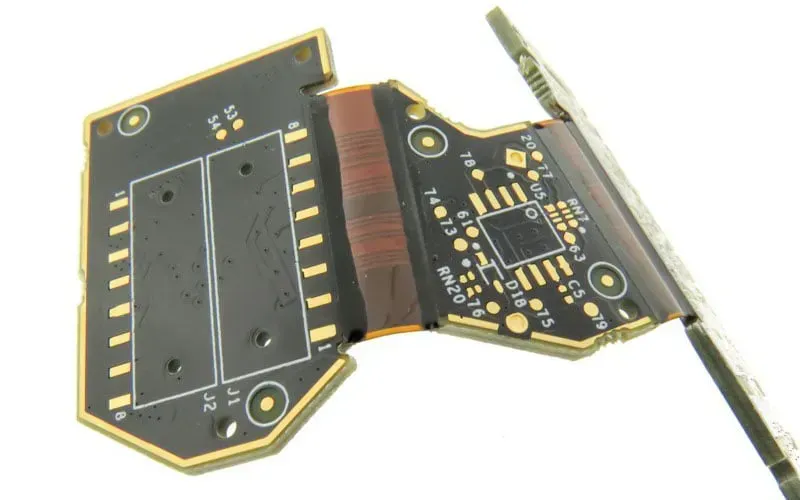
Flexible PCB Board Bending
In the realm of wearable health monitoring bracelets, the physical constraints of form factor and the dynamic nature of user interaction necessitate innovative PCB solutions. Rigid-flex and flexible PCBs stand out as the preferred technologies, offering unparalleled advantages in conforming to irregular geometries, enduring repetitive motion, and significantly reducing both size and weight. These advanced PCB types are instrumental in enabling the sleek, comfortable, and highly functional designs that define modern wearable health devices, ensuring reliable performance even under strenuous conditions.
Feature
Rigid-Flex PCB Benefits
Flexible PCB Benefits
Space Efficiency
Integrates rigid and flexible sections, eliminating connectors and saving space.
Allows for compact designs, bending to fit tight enclosures and complex shapes, reducing overall footprint by up to 60% compared to rigid PCBs.
Minimizes wiring and board size, often enabling smaller, lighter devices by reducing mechanical connectors and associated cabling.
Attribute
Rigid-Flex PCB
Flexible PCB
Durability
Enhanced mechanical stability with integrated rigid sections, capable of withstanding moderate bending cycles.
Exceptional resilience to repeated bending, vibration, and shock, suitable for highly dynamic applications like wearable joints.
Highly resistant to vibration and shock, maintaining integrity under constant movement.
How do rigid-flex PCBs enhance reliability in wearable health monitoring bracelets? Rigid-flex PCBs significantly enhance reliability by integrating rigid sections for component mounting and flexible sections for interconnections. This eliminates the need for separate wires and connectors, reducing potential points of failure, improving signal integrity, and enhancing resistance to environmental factors like vibration and impact, which are common in wearable applications. The unified structure ensures robust electrical connections over the device's lifespan.
What are the key manufacturing considerations for flexible PCBs in wearables? Key manufacturing considerations for flexible PCBs include the selection of appropriate flexible dielectric materials (e.g., polyimide), specialized etching processes to prevent material stress, and careful handling to prevent creases or damage during assembly. Precise routing and controlled impedance are crucial for maintaining signal integrity in dynamic environments. Zero One Solution Limited employs specialized processes to ensure the integrity and performance of these delicate boards.
Can rigid-flex PCBs support high-density component placement? Yes, rigid-flex PCBs are well-suited for high-density component placement, especially in their rigid sections. This allows for the integration of complex circuits and numerous components (e.g., biosensors, microcontrollers, communication modules) within a compact footprint. The flexible sections then provide efficient and space-saving routing pathways to different parts of the wearable device, optimizing overall design and functionality while minimizing size.
Ensuring Reliability and Durability in Wearable PCB Manufacturing
Quality Control Testing Equipment
For wearable health monitoring bracelets, the PCB is not merely a circuit board; it's the resilient core that must withstand constant exposure to dynamic environments, including sweat, physical movement, and varying temperatures. Ensuring the long-term reliability and durability of these PCBs is paramount, directly impacting device functionality, user safety, and brand reputation. At Zero One Solution Limited, our manufacturing processes, material selections, and rigorous testing protocols are meticulously engineered to exceed the demanding performance requirements of wearable technology, guaranteeing optimal performance and longevity for every Wearable Health Monitoring Bracelet PCB Solution.
Aspect
Challenge in Wearables
Zero One Solution's Approach
Material Selection
Biocompatibility, flexibility, resistance to moisture and chemicals (e.g., sweat)
Utilizing advanced substrates like polyimide (PI) for flexibility and epoxy-based laminates with low moisture absorption; selecting lead-free and RoHS compliant materials for user safety and environmental compliance. Strategic use of conformal coatings for additional protection.
Manufacturing Processes
Miniaturization, high-density interconnections, reliable solder joints for small components, consistent quality across high volumes
Implementing advanced automated assembly lines (SMT, SMT/THT) with precise pick-and-place machines for fine-pitch components; employing stringent solder paste inspection (SPI) and automated optical inspection (AOI) to ensure flawless connections. Specializing in rigid-flex and flexible PCB fabrication to meet complex form factors.
Environmental Protection
Exposure to sweat, humidity, dust, and temperature fluctuations
Applying moisture-resistant and anti-corrosion coatings (e.g., Parylene, epoxy, acrylic) and encapsulants to protect sensitive components. Designing PCBs with optimized thermal management to dissipate heat effectively, preventing performance degradation.
What IPC standards are crucial for wearable health monitoring bracelet PCBs? For wearable health monitoring bracelet PCBs, adherence to IPC standards is vital for quality and reliability. Key standards include IPC-6012 (Qualification and Performance Specification for Rigid Printed Boards), IPC-6013 (Qualification and Performance Specification for Flexible/Rigid-Flex Printed Boards) for the board itself, and IPC-A-610 (Acceptability of Electronic Assemblies) for the assembly process. Additionally, IPC-J-STD-001 (Requirements for Soldered Electrical and Electronic Assemblies) dictates soldering quality. Zero One Solution strictly adheres to these standards to ensure the highest quality and consistent performance, tailored for the unique demands of wearable devices such as the Wearable Health Monitoring Bracelet PCB Solution, minimizing defects and maximizing durability.
Future Trends in Wearable Health Monitoring and PCB Innovations
The landscape of wearable health monitoring is undergoing a profound transformation, driven by advancements in sensor technology, artificial intelligence, and sophisticated data analytics. These innovations are reshaping the demands on Wearable Health Monitoring Bracelet PCB Solutions, requiring increasingly complex, miniaturized, and highly integrated designs. As a veteran SEO engineer and marketing expert, I foresee a future where these devices move beyond simple data collection to offer predictive health insights, personalized interventions, and seamless integration into our daily lives, fundamentally altering how we manage personal health. This evolution necessitates continuous innovation in PCB design and manufacturing to accommodate emerging technologies while maintaining the critical balance of performance, power efficiency, and durability.
AI Integration in Wearables Artificial intelligence and machine learning are becoming integral to wearable health monitoring, enabling on-device data processing for real-time anomaly detection, predictive analytics, and personalized health coaching. This necessitates PCBs capable of supporting powerful edge AI chipsets, optimized for low power consumption and high computational efficiency within a compact form factor. Future PCBs will feature dedicated AI accelerators and enhanced memory interfaces to handle the increasing demands of AI algorithms directly on the bracelet, reducing reliance on cloud processing and improving response times, ultimately enhancing the efficacy of the Wearable Health Monitoring Bracelet PCB Solution.
Advanced Multi-Sensor Fusion The next generation of wearable health bracelets will incorporate an even broader array of sensors, fusing data from multiple sources (e.g., optical, electrical, acoustic, chemical) to provide a more comprehensive and accurate picture of physiological states. This trend demands highly integrated PCBs that can efficiently manage diverse sensor interfaces, minimize crosstalk, and ensure signal integrity across various modalities. The design challenge lies in routing complex signal paths in confined spaces, requiring advanced multi-layer PCBs and sophisticated electromagnetic compatibility (EMC) strategies for the Wearable Health Monitoring Bracelet PCB Solution to prevent interference and maintain data accuracy.
Non-Invasive Continuous Monitoring The focus is shifting towards continuous, non-invasive monitoring of a wider range of biomarkers, moving beyond traditional heart rate and step counting. Innovations like continuous glucose monitoring (CGM) through non-invasive means, blood pressure sensing from the wrist, and even stress hormone detection are on the horizon. These technologies will require highly sensitive and precise sensor integration on the PCB, often utilizing novel materials and micro-fabrication techniques to achieve clinical-grade accuracy in a discreet and comfortable form factor, pushing the boundaries of the Wearable Health Monitoring Bracelet PCB Solution.
Future Trend
Impact on PCB Design
Zero One Solution's Readiness
Micro-LED Displays
Requires ultra-fine pitch interconnects, high-density routing, and advanced thermal management due to increased pixel density and brightness.
Proficient in high-density interconnect (HDI) PCBs, advanced stacking technologies, and thermal dissipation solutions to support next-gen display integration for Wearable Health Monitoring Bracelet PCB Solution applications.
What are the key considerations for integrating AI into a Wearable Health Monitoring Bracelet PCB Solution? Integrating AI into a wearable PCB requires careful consideration of computational power, energy efficiency, and thermal management. The PCB must accommodate specialized AI processors or neural processing units (NPUs) that can perform complex algorithms with minimal power consumption, crucial for battery-powered devices. Additionally, compact designs need efficient heat dissipation solutions to prevent performance degradation. Optimizing trace routing for high-speed data transfer between the NPU, sensors, and memory is also paramount to ensure real-time processing and effective AI functionality.
Zero One Solution Limited remains at the forefront of these advancements, continuously investing in cutting-edge manufacturing capabilities and R&D to support the evolving demands of Wearable Health Monitoring Bracelet PCB Solutions. Our expertise in rigid-flex PCBs, high-density interconnect (HDI) technology, and advanced material selection positions us to meet the intricate requirements of future wearable devices, ensuring our clients can rapidly prototype and scale their most innovative health monitoring solutions.
The journey from concept to a market-ready wearable health monitoring bracelet is complex, yet immensely rewarding. At its core lies the need for a meticulously engineered PCB solution that can withstand the rigors of daily wear while delivering consistent, accurate data. Zero One Solution Limited, with our deep expertise in rapid prototyping, PCB design, manufacturing, and assembly, stands as your trusted partner in navigating this intricate landscape. We are committed to empowering innovators like you to push the boundaries of health technology, offering comprehensive one-stop services that streamline your development cycle and ensure your product excels. Don't let PCB complexities be a barrier to your vision; connect with Zero One Solution Limited today and let's transform your wearable health monitoring dreams into reality.