Wireless Communication Antenna Matching Network PCB Solution
2025.08.08
In the dynamic landscape of wireless communication, the efficiency and reliability of signal transmission are paramount. At the heart of this challenge lies the antenna matching network – a critical component that bridges the gap between transceiver and antenna. A perfectly tuned matching network on a meticulously designed Printed Circuit Board (PCB) can transform a good wireless device into an exceptional one, ensuring maximum power transfer and minimal signal loss. For innovators striving to accelerate product development and deliver superior wireless performance, understanding and implementing robust PCB solutions for these networks is not just an advantage, but a necessity. Zero One Solution Limited, with its deep expertise in rapid-response R&D prototype manufacturing, offers a comprehensive one-stop service from design to assembly, empowering clients to achieve unparalleled efficiency in bringing their innovative solutions to market.
The Critical Role of Antenna Matching Networks in Wireless Communication
In the intricate world of wireless communication, the antenna matching network stands as a linchpin for achieving optimal signal integrity, efficient power transfer, and superior overall system performance. A meticulously designed matching network ensures that the impedance of the antenna is precisely matched to that of the transmitter or receiver, maximizing power delivery and minimizing signal reflections. This critical alignment is not merely an engineering ideal but a fundamental prerequisite for reliable wireless operation, directly impacting range, data rates, battery life, and compliance with regulatory standards. Without it, even the most advanced wireless systems would suffer from debilitating losses, rendering their intended functionalities severely compromised.
The repercussions of a mismatched antenna network extend far beyond minor performance dips. When impedances are not aligned, a significant portion of the transmitted power is reflected back towards the source, a phenomenon quantified by the Voltage Standing Wave Ratio (VSWR). A high VSWR indicates poor matching, leading to reduced effective radiated power (ERP), diminished signal-to-noise ratio (SNR), and potentially overheating of power amplifiers. For receivers, a mismatch results in less signal power reaching the input, degrading sensitivity and making it harder to decode weak signals. Therefore, the precise design and implementation of antenna matching networks are not just about efficiency but about the fundamental viability and reliability of any wireless communication PCB solution, demanding expert knowledge in RF theory, PCB material science, and advanced simulation techniques.
Key Principles of RF PCB Design for Matching Networks
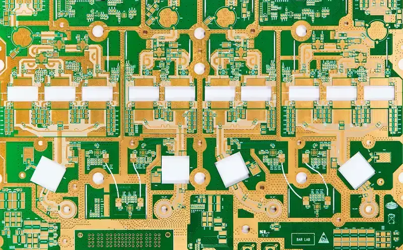
RF PCB Design Diagram
Effective antenna matching network PCB design is paramount for optimal wireless communication system performance, as even minor design oversights can lead to significant signal degradation and power loss. This section unpacks the foundational principles crucial for engineering high-frequency RF PCBs that precisely integrate antenna matching networks, ensuring maximum power transfer and signal integrity. Adhering to these principles, including rigorous impedance control, strategic trace geometries, judicious material selection, robust ground plane considerations, and meticulous component placement, is non-negotiable for achieving reliable and efficient wireless communication.
Impedance Control Maintaining a consistent characteristic impedance (typically 50 ohms) throughout the RF signal path is critical. Mismatches lead to reflections (VSWR), reducing power delivered to the antenna. This requires precise trace width, dielectric constant, and board thickness control, often utilizing controlled impedance traces like microstrip or stripline configurations. Advanced simulation tools are indispensable for verifying impedance profiles.
Trace Geometries The physical dimensions and routing of RF traces directly impact performance. Short, straight traces minimize parasitic inductance. Bends should be gradual (e.g., 45-degree or arc bends) to avoid impedance discontinuities. Differential pairs require precise length and spacing matching to preserve common-mode rejection and signal integrity at high frequencies, critical for balancing and optimizing RF transmission.
Design Aspect
Key Consideration for RF PCB
Impact on Performance
Material Selection
Low-loss dielectric materials (e.g., Rogers, Taconic) with stable dielectric constant (Dk) and low dissipation factor (Df).
Minimizes signal attenuation and phase distortion, especially at higher frequencies, ensuring efficient power transfer.
Ground Plane Considerations A solid, continuous ground plane is essential for providing a stable reference voltage, minimizing electromagnetic interference (EMI), and controlling impedance. Breaks or slots in the ground plane under RF traces can disrupt current return paths, leading to noise and impedance mismatches. Vias should be strategically placed to ensure robust ground connections and minimize inductance, effectively creating a "quiet" RF environment.
Design Aspect
Key Consideration for RF PCB
Impact on Performance
Component Placement
Shortest possible trace lengths, direct connections, minimizing via usage, and careful thermal management for RF components.
Reduces parasitic effects (inductance/capacitance), minimizes signal loss and distortion, and prevents thermal runaway, enhancing overall reliability and performance.
Common Antenna Matching Network Topologies and Their PCB Implementations
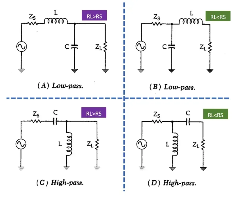
L-Network Matching Circuit Board
Achieving optimal power transfer and minimizing signal reflections in wireless communication systems hinges on the effective implementation of antenna matching networks. These networks, designed to transform the antenna's impedance to match the impedance of the transmission line or RF front-end, are critical for maximizing radiated power and receiver sensitivity. Various topologies exist, each with specific advantages and considerations for their realization on a Printed Circuit Board (PCB), where component selection, layout precision, and parasitic management are paramount for high-frequency performance.
L-Network The L-network is the simplest matching network topology, consisting of two reactive components (capacitors and/or inductors) arranged in an 'L' shape. It can match any complex impedance to a real impedance. Its simplicity makes it cost-effective and space-efficient on a PCB, ideal for applications where component count and board space are limited. However, its fixed Q (quality factor) limits its versatility, making it suitable for narrow-band applications where the impedance variation is minimal. PCB implementation requires careful placement of components to minimize parasitic inductance and capacitance, especially at higher frequencies, and ensuring short, wide traces for low impedance connections.
Pi-Network The Pi-network comprises three reactive components, typically two capacitors and one inductor, forming a 'Pi' shape. This topology offers greater flexibility than the L-network due to its three adjustable components, allowing for independent control over both impedance transformation and Q-factor. This makes it highly suitable for wider bandwidth applications or situations where a precise Q is required. On a PCB, the Pi-network generally occupies more space due to the additional component. Careful layout is needed to avoid mutual coupling between the components and to maintain short connections to minimize trace inductance, which can significantly impact performance at RF frequencies.
T-Network Similar to the Pi-network, the T-network also uses three reactive components, usually two inductors and one capacitor, arranged in a 'T' shape. Like the Pi-network, it provides excellent flexibility in matching a wide range of impedances and offers control over the Q-factor. T-networks are often preferred in scenarios where series inductance is beneficial or when dealing with higher impedance transformations. From a PCB implementation perspective, the T-network also demands careful layout to manage component sizes and parasitic effects. The physical separation of components and optimized trace routing are crucial to ensure that the network performs as designed, especially considering the impact of PCB substrate properties on component values and performance.
Topology
Components
Flexibility (Q-factor)
PCB Space Requirement
Ideal Application
L-Network
2 (L, C)
Limited (Fixed)
Minimal
Narrow-band, cost-sensitive
Pi-Network
3 (L, C)
High (Adjustable)
Moderate
Wide-band, precise Q control
T-Network
3 (L, C)
High (Adjustable)
Moderate
High impedance transformation, specific series inductance needs
Challenges in Antenna Matching Network PCB Development and How to Overcome Them
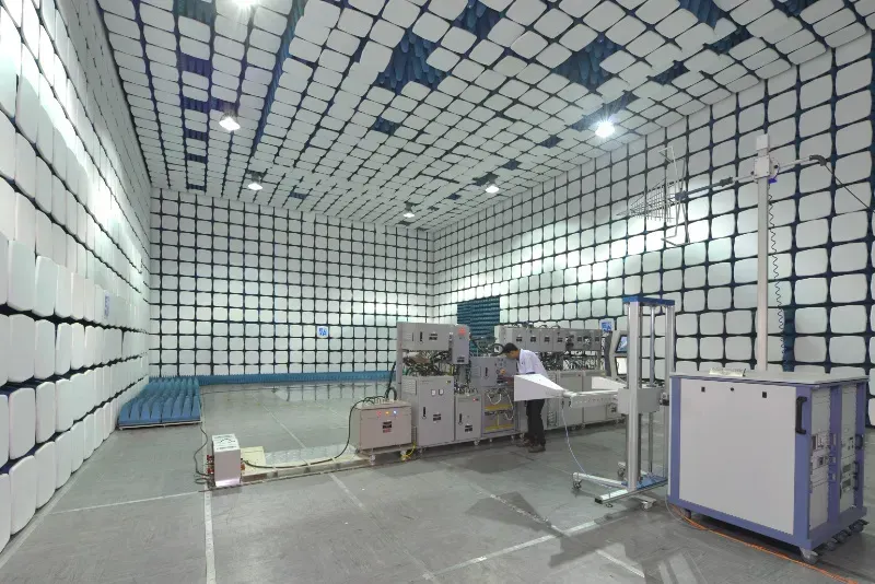
EMI Testing Laboratory
Developing antenna matching network PCBs for wireless communication systems presents a unique set of engineering challenges, primarily due to the stringent requirements of high-frequency RF performance. Overcoming these hurdles is critical for achieving optimal signal integrity, maximizing power transfer, and ensuring the overall reliability and efficiency of wireless devices. The complexities range from inherent manufacturing variations and unpredictable component behaviors to pervasive electromagnetic interference and crucial thermal management, all of which directly impact the functionality of the matching network and, by extension, the entire communication link. Addressing these issues systematically through robust design methodologies and advanced manufacturing practices is paramount to successful deployment.
How do manufacturing tolerances affect Antenna Matching Network PCB performance? Manufacturing tolerances introduce slight variations in trace dimensions, dielectric constants, and substrate thickness, which directly impact impedance control and the resonant frequency of the matching network. Even minor deviations can lead to significant impedance mismatches at high frequencies, resulting in increased signal reflection (VSWR) and reduced power transfer. To overcome this, designers should incorporate robust design rules, such as wider traces where possible to minimize the impact of etching variations, and utilize PCB manufacturers with tight process controls and advanced fabrication capabilities that can consistently meet stringent impedance specifications (e.g., ±5%). Post-fabrication tuning options, like adjustable components, can also compensate for residual variations.
What challenges does component variability pose in wireless communication antenna matching networks? Passive components (capacitors, inductors) used in antenna matching networks exhibit inherent manufacturing tolerances, temperature dependencies, and parasitic effects that cause their actual values to deviate from nominal specifications, especially at RF frequencies. This variability can shift the network's intended resonant frequency and impedance transformation. Mitigating this requires selecting high-Q components with tight tolerances (e.g., 1% or 0.5% tolerance) and stable temperature coefficients. Incorporating tuneable components or providing test points for network analysis during prototyping allows for empirical adjustment to compensate for component variations and optimize performance in the final assembly.
How can electromagnetic interference (EMI) be managed in Antenna Matching Network PCBs? Electromagnetic interference (EMI) can degrade antenna matching network performance by inducing unwanted currents, altering impedance characteristics, and injecting noise into the signal path. Sources include adjacent digital circuitry, power supplies, and external RF sources. Effective EMI management involves strategic PCB layout practices such as proper ground plane stitching to create a solid, low-impedance return path, shielding sensitive traces with guard bands or via fences, and carefully routing RF traces away from noisy digital lines. Using appropriate filtering at power entry points and selecting components with low EMI signatures also contributes to a cleaner RF environment.
Why is thermal management critical for high-frequency antenna matching networks? High-frequency signals passing through matching network components can generate heat due to ohmic losses, dielectric losses, and component dissipation. Elevated temperatures can alter the electrical properties of components (e.g., capacitance, inductance, dielectric constant of the substrate), causing the matching network to detune and leading to performance degradation, increased VSWR, and reduced power efficiency. Effective thermal management involves selecting components rated for higher operating temperatures, using low-loss PCB materials, incorporating thermal vias to dissipate heat from components to ground planes, and ensuring adequate airflow or heatsinking, especially in high-power applications.
What role does simulation play in overcoming PCB development challenges? RF simulation tools (e.g., ADS, CST, HFSS) are indispensable for predicting and mitigating challenges in antenna matching network PCB development. They allow engineers to model trace impedances, analyze electromagnetic fields, simulate component parasitics, and predict network performance (VSWR, insertion loss) before physical fabrication. This virtual prototyping identifies potential issues like impedance mismatches, coupling effects, and EMI hotspots early in the design cycle, significantly reducing costly design iterations, accelerating time-to-market, and ensuring optimal RF performance from the outset.
Zero One Solution Limited's Expertise in High-Frequency PCB Solutions
High-Frequency PCB Production Line
Zero One Solution Limited stands at the forefront of high-frequency PCB solutions, particularly for the intricate demands of wireless communication antenna matching networks. Our deep expertise, honed over a decade in the industry, ensures that every PCB we design and manufacture delivers unparalleled precision and performance, critical for optimal signal integrity and power transfer in complex RF environments. We empower clients to accelerate their product development cycles with our robust capabilities, making us a trusted partner in the global PCBA supply chain.
Advanced Manufacturing Capabilities We leverage state-of-the-art manufacturing equipment and processes specifically optimized for high-frequency materials and trace geometries. This includes precision laser drilling, advanced etching techniques, and controlled impedance fabrication to minimize signal loss and maintain design integrity for sensitive RF circuits. Our facilities in Shenzhen, China, are equipped with the latest technology for producing complex multi-layer PCBs with tight tolerances.
Experienced RF Engineering Team Our team comprises veteran RF and PCB design engineers with extensive experience in Silicon Valley, possessing a profound understanding of electromagnetic theory, transmission line effects, and parasitic capacitance/inductance. This expertise is crucial for designing and optimizing antenna matching networks, ensuring that theoretical models translate seamlessly into practical, high-performance PCB layouts. We meticulously analyze impedance matching, S-parameters, and radiation patterns to achieve peak performance.
Rigorous Quality Control and Testing Quality is paramount in high-frequency PCB manufacturing. Zero One Solution Limited implements a stringent multi-stage quality control process, from material selection verification to in-process inspections and final functional testing. We utilize advanced testing equipment, including Vector Network Analyzers (VNAs) and Time-Domain Reflectometers (TDRs), to meticulously verify impedance control, insertion loss, return loss, and other critical RF parameters, guaranteeing robust and reliable performance for every board.
Our commitment to excellence and innovation is further exemplified by our rapid prototyping service. Recognizing the critical need for speed in R&D, we offer expedited production timelines without compromising on quality or precision. This capability significantly reduces time-to-market for our clients, enabling faster iteration and validation of designs. Our strategic presence in Shenzhen and Dubai ensures global reach and localized support, providing seamless access to our world-class PCB solutions.
Our One-Stop Service: From Design to Assembly for Seamless Integration
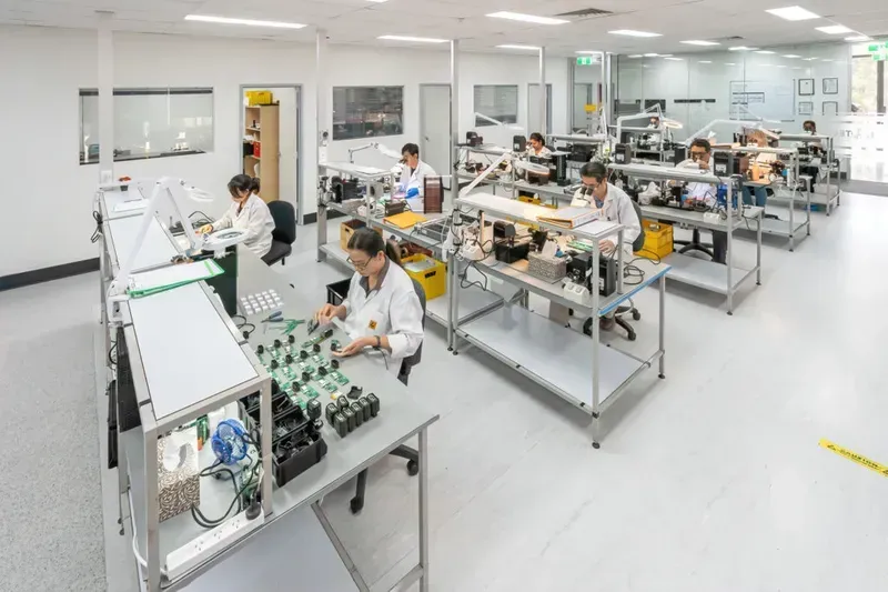
PCB Assembly Workshop
At Zero One Solution Limited, we understand that bringing a wireless communication product to market requires more than just a well-designed antenna matching network PCB. It demands a holistic approach, from initial concept to final assembly. Our one-stop service offers a seamless, integrated solution that encompasses every stage of PCB development: meticulous design, precision manufacturing, and expert assembly. This streamlined process is engineered to significantly reduce lead times, optimize costs, and guarantee unwavering quality, providing a distinct competitive advantage for complex antenna matching network PCB solutions.
Integrated Workflow for Efficiency By consolidating PCB design, manufacturing, and assembly under one roof, we eliminate the common pitfalls associated with fragmented supply chains. This integration ensures consistent communication, reduces coordination overhead, and minimizes the risk of errors, accelerating your time-to-market.
Accelerated Product Development Our rapid prototyping capabilities, combined with an integrated workflow, allow for iterative design improvements and quick validation cycles. This agility is crucial for wireless communication projects where timely iteration and validation of antenna matching networks can significantly impact project success.
Cost Optimization and Transparency A unified service model allows for greater cost control and transparency. Clients avoid hidden costs associated with multiple vendors and benefit from optimized material procurement and manufacturing processes, leading to overall project cost efficiencies.
Uncompromised Quality Assurance Quality control is integrated at every stage. Our experienced engineers oversee the entire process, from ensuring design integrity for high-frequency applications to implementing rigorous testing during manufacturing and assembly. This end-to-end quality assurance is vital for the performance and reliability of sensitive antenna matching networks.
Expertise in Complex RF PCB Solutions Our specialized expertise in high-frequency RF PCB solutions, including advanced material selection and precise impedance control, is applied throughout the entire design and manufacturing process. This ensures that the delicate requirements of wireless communication antenna matching networks are met with utmost precision.
Scalability from Prototype to Production Whether you require a few prototype boards for testing or large-scale production, our one-stop service scales with your needs. We maintain consistent quality and efficiency across all volumes, providing a reliable partner for your entire product lifecycle.
The demands of modern wireless communication necessitate precision and expertise at every stage of development, particularly in the critical area of antenna matching networks and their underlying PCB solutions. Zero One Solution Limited stands as your ideal partner, offering a holistic, one-stop service from initial design to final assembly, backed by over a decade of industry leadership and a global supply chain network. Our commitment to rapid prototyping and uncompromising quality empowers you to accelerate your product development cycles, reduce time-to-market, and achieve optimal wireless performance. By choosing Zero One Solution Limited, you're not just selecting a PCB provider; you're investing in a collaborative partnership dedicated to transforming your innovative concepts into market-ready realities. Contact us today to discuss your next wireless communication project and experience the Zero One Solution Limited difference.