Imagine a world where voltage levels fluctuate wildly, causing havoc in sensitive electronic circuits. The Zener diode, a seemingly simple semiconductor device, is engineered to address this precise problem. Unlike typical diodes that block reverse current, the zener diode is designed to allow current to flow in the reverse direction when a specific voltage is reached, offering a stable voltage reference, a vital function in so many electronic devices, in this article, we will delve into the workings of zener diodes, exploring their functions, applications, and significance in modern circuitry, and discover how this critical component contributes to the smooth operation of countless everyday devices.
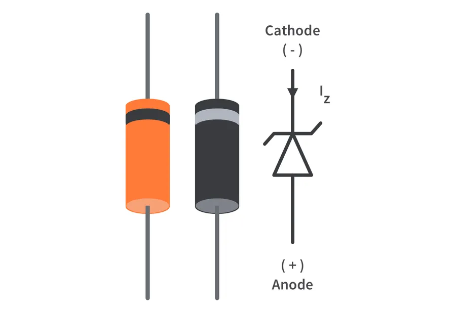
Zener diodes are semiconductor devices engineered to conduct current in the reverse direction when the applied reverse voltage reaches a specific threshold, known as the Zener voltage. This behavior is fundamentally different from standard diodes, which primarily block reverse current. The ability of Zener diodes to operate in the reverse bias breakdown region is achieved through a heavily doped p-n junction, setting them apart for voltage regulation and protection applications.
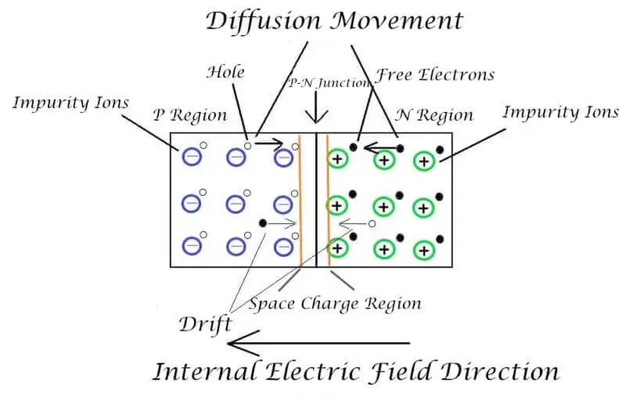
Zener breakdown is a quantum mechanical phenomenon that occurs in heavily doped p-n junctions under reverse bias conditions. Unlike avalanche breakdown, which is caused by impact ionization, Zener breakdown occurs when a strong electric field directly extracts electrons from the valence band to the conduction band within the depletion region. This effect creates a significant increase in reverse current with minimal change in voltage, enabling the Zener diode's unique voltage regulation capabilities. The high doping concentrations result in a narrow depletion region and a strong electric field, facilitating this tunneling effect.
The primary factors influencing Zener breakdown are the doping concentration and the resulting electric field strength. Higher doping levels lead to a narrower depletion region and, consequently, a more intense electric field for a given reverse bias voltage. This higher electric field is crucial for facilitating the tunneling of electrons. The temperature also has a minor effect on the Zener voltage, with the voltage typically decreasing slightly as temperature rises.
It's crucial to distinguish between Zener breakdown and avalanche breakdown, although both mechanisms result in reverse current flow. Avalanche breakdown relies on high-energy carriers colliding with atoms, creating additional free electrons and holes in a chain reaction. This process typically occurs at higher reverse voltages than Zener breakdown and is characteristic of lightly doped junctions. Zener breakdown, being a tunneling effect, dominates at lower reverse voltages in heavily doped junctions. In practical Zener diodes, both effects may contribute to the overall breakdown behavior, but one mechanism tends to be dominant based on the diode's doping.
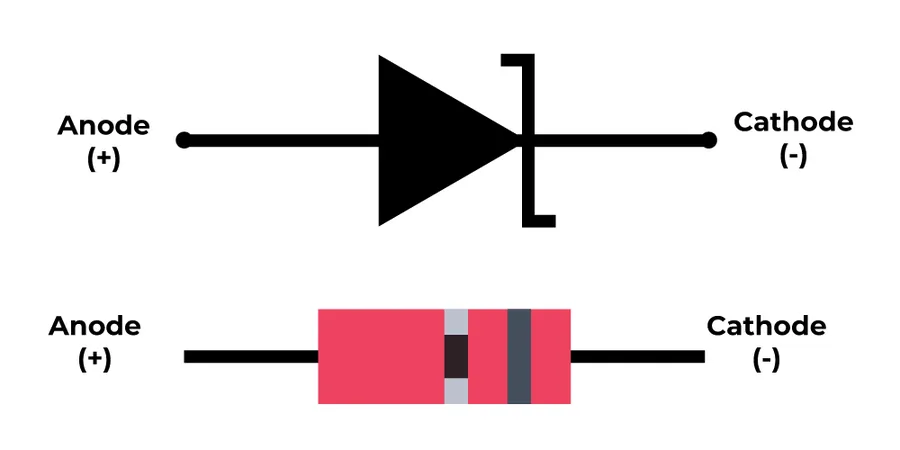
The Zener diode, distinguished by its unique reverse-bias operating characteristic, employs a specific circuit symbol and construction to achieve its functionality. Understanding these elements is fundamental to correctly interpreting and designing circuits incorporating Zener diodes.
The Zener diode symbol is similar to that of a standard diode but includes angled extensions on the cathode side. These extensions visually represent the diode’s specialized reverse-bias breakdown behavior.
Zener diodes are constructed using a heavily doped P-N junction. The doping concentration is significantly higher than that of a standard diode. This heavy doping is crucial for achieving a precisely defined reverse breakdown voltage, known as the Zener voltage. The high doping level creates a narrow depletion region, allowing for electron tunneling and subsequent current conduction under reverse bias at a consistent voltage.
Zener diodes are available in various package types, including through-hole and surface-mount packages. Common package styles include DO-35, DO-41, SOD-123, and SOT-23. The chosen package not only determines how the diode can be mounted, but also impacts its ability to dissipate heat. Higher power Zener diodes require packaging that facilitates effective thermal management, such as larger packages or heat sinks, to prevent damage from excessive heat generation.
Thermal considerations are paramount in Zener diode applications. The reverse breakdown process generates heat, particularly when the diode is operating close to its rated current and power limits. Incorrect thermal management can lead to overheating, reduced performance, and even permanent damage to the diode. Designers must carefully choose a Zener diode with an appropriate power rating and utilize thermal management techniques, such as heat sinks, where necessary, to ensure the stability and longevity of the circuit.
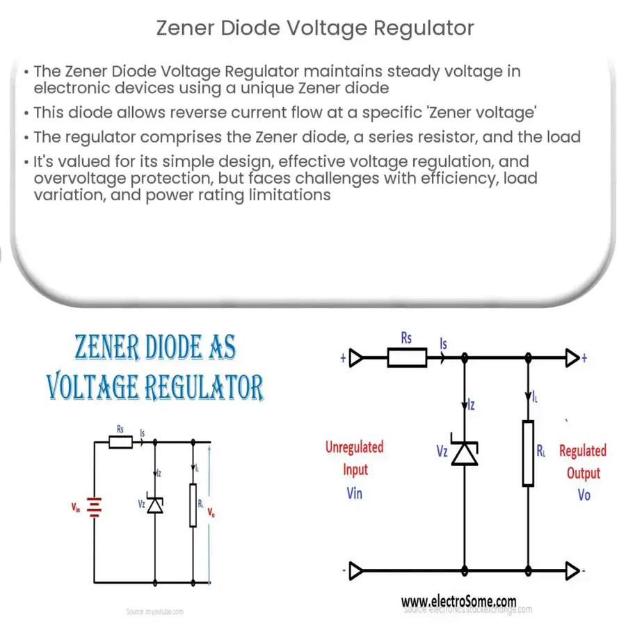
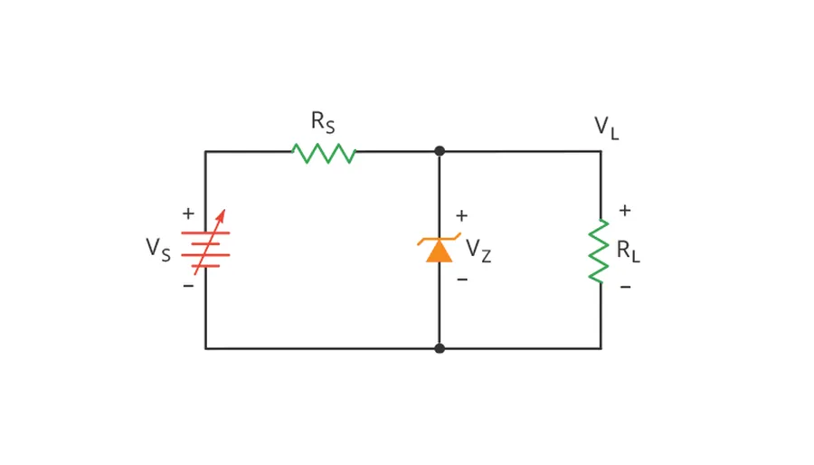
Zener diodes are frequently employed as voltage regulators, leveraging their unique ability to maintain a nearly constant voltage across their terminals when operating in the reverse breakdown region. This characteristic allows for the creation of simple and effective voltage regulation circuits, crucial in numerous electronic applications where a stable voltage supply is required despite fluctuations in input voltage or load current.
The core principle of a Zener diode voltage regulator involves connecting the Zener diode in parallel with the load, and in series with a current-limiting resistor. The resistor limits the current flowing through the diode and protects it from overcurrent damage. The Zener diode will then conduct current once the reverse voltage across it reaches its Zener voltage, diverting excess current to maintain a constant voltage across the load.
The Zener diode acts like a shunt regulator, which means it diverts excess current when the input voltage is above the Zener voltage, this shunting action prevents excessive voltage from reaching the load. The load and the Zener diode effectively 'share' the current flow, the Zener diode conducting more current as the load current decreases and input voltage increases and vice versa. This self adjusting mechanism helps maintain consistent voltage regulation under variable load conditions.
| Parameter | Description |
|---|---|
| Zener Voltage (Vz) | The reverse voltage at which the Zener diode begins to conduct significantly. |
| Current Limiting Resistor (Rs) | Limits current flow, protecting the Zener diode and providing stable output, needs to be sized properly for the load requirements. |
| Load Resistance(Rl) | The load on the output of the regulator can be a variable resistance, the current shunted by the diode is dependent on this value and the input voltage. |
| Input Voltage (Vin) | The unregulated input voltage, usually higher than the desired output voltage, the regulation is dependent on this variable. |
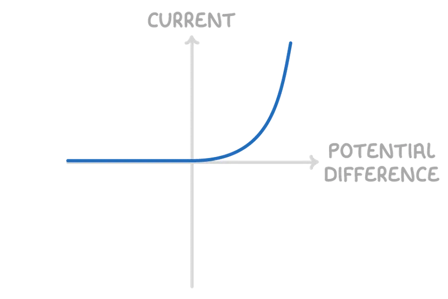
The voltage-current (V-I) characteristic curve of a Zener diode is fundamental to understanding its operation, especially in reverse bias. This curve distinctly illustrates the Zener diode's behavior in three primary regions: forward bias, reverse blocking, and Zener breakdown. Analyzing this curve provides crucial insights into how a Zener diode maintains a stable voltage.
| Region | Voltage | Current | Behavior | Key Points |
|---|---|---|---|---|
| Forward Bias | Positive voltage applied to anode | Current increases exponentially with voltage | Behaves like a standard diode | Typical forward voltage drop around 0.7V for silicon |
| Reverse Blocking | Reverse voltage applied to anode, below Zener voltage | Minimal current flow (leakage current) | Diode is effectively non-conducting | Leakage current is very small, ideally zero |
| Zener Breakdown | Reverse voltage exceeds Zener voltage | Rapid increase in reverse current | Diode maintains a relatively constant voltage | Zener voltage (Vz) and the knee of breakdown are important parameters |
The 'knee' of the Zener breakdown region on the V-I curve is where the reverse current begins to increase rapidly. This point also marks the Zener voltage (Vz) which is the critical operating point for voltage regulation. The sharpness of this knee is a crucial characteristic, indicating how precisely the diode will maintain a constant voltage.
Zener diodes, due to their unique reverse breakdown characteristic, are indispensable in various electronic applications. They provide a stable voltage reference, protect circuits from over-voltage conditions, and enable precise voltage clipping and regulation. Their versatility makes them a fundamental component in many electronic designs, ranging from simple circuits to complex systems.
This section addresses common queries regarding Zener diodes, providing clear and concise answers to enhance understanding and practical application of these specialized diodes.
While both Zener and standard diodes are semiconductor devices that allow current to flow primarily in one direction, their behavior under reverse bias is fundamentally different, leading to distinct applications. This section will provide a detailed comparison of their characteristics, construction, and operation.
| Feature | Zener Diode | Standard Diode |
|---|---|---|
| Primary Function | Voltage regulation, voltage reference, over-voltage protection | Rectification, signal processing |
| Reverse Bias Behavior | Designed to operate in reverse breakdown region at a specific Zener voltage | Blocks current in reverse bias until breakdown (typically destructive) |
| Doping Level | Heavily doped p-n junction | Lightly doped p-n junction |
| Breakdown Mechanism | Zener effect (quantum mechanical tunneling) or avalanche breakdown, depending on the voltage | Avalanche breakdown |
| Breakdown Voltage | Precisely controlled and specified | Variable, often not specified and not designed to be operated under reverse breakdown. |
| Forward Voltage Drop | Similar to standard diode (~0.7V for silicon) | Typically ~0.7V for silicon |
| Applications | Voltage regulators, over-voltage protection circuits, voltage clipping, reference voltage circuits. | Rectifiers, signal diodes, flyback diodes |
| Symbol | Similar to standard diode but with bent cathode ends | Standard diode symbol (triangle pointing to a line) |
| Limitations | Limited power handling capability without additional components; may have a degree of voltage variation with temperature and current. | Not designed for voltage regulation; subject to permanent damage if reverse breakdown voltage is exceeded. |
Selecting the appropriate Zener diode is crucial for achieving desired circuit performance and reliability. The selection process involves careful consideration of several key parameters that directly impact the diode's behavior within a specific application. These parameters include Zener voltage, power dissipation rating, and tolerance, each playing a vital role in ensuring the diode operates within its safe and effective limits. Ignoring these criteria can lead to improper circuit function, component damage, or even catastrophic failure.
In conclusion, the Zener diode's unique reverse breakdown behavior is fundamental to its role as a precision voltage controller. From stabilizing voltages in power supplies to providing critical protection against voltage surges, Zener diodes are essential in ensuring stable performance of all sorts of electronics. By understanding their characteristics and applications, engineers and hobbyists alike can leverage the power of zener diode technology in countless practical and innovative designs, advancing the very fabric of the technological world around us.

