
As LiDAR technology scales, the physical constraints of sensor hardware become the primary bottleneck for system performance. Balancing high-density interconnects with the mechanical demands of rigid-flex circuits requires a nuanced approach to DFM. In this guide, we navigate the critical engineering decisions that define reliable, high-frequency LiDAR systems.
Understanding the LiDAR Interconnect Challenge
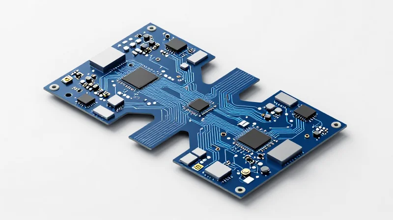
The Complexity of Rigid-Flex LiDAR Interconnects
LiDAR sensors demand a unique architectural approach because they must balance dense high-frequency signal processing with the mechanical requirements of a flexible interconnect. Unlike standard industrial electronics, these systems face dual pressures: maintaining low-loss transmission at millimeter-wave frequencies while ensuring mechanical fatigue resistance during vibration or physical integration. The rigid-flex transition creates a primary point of failure where impedance discontinuities can severely degrade signal integrity and thermal dissipation.
Critical Performance Metrics Comparison
| Parameter | Standard Industrial PCB | High-Frequency LiDAR Rigid-Flex |
|---|---|---|
| Frequency Range | Low (< 1 GHz) | High (> 24 GHz) |
| Thermal Tolerance | Moderate | Extreme/High Density |
| Flex Reliability | N/A | High Fatigue Resistance Required |
| Impedance Control | Standard +/- 10% | Tight +/- 5% or better |
Key Challenges in Advanced LiDAR DFM
- How does signal loss manifest at high frequencies?
At LiDAR frequencies, even minor variances in trace width or dielectric constant within the flex portion cause signal reflection and phase shift, leading to data inaccuracy. - Why is thermal management more difficult for rigid-flex?
The transition areas limit heat sinking capacity; if the stack-up is not optimized for thermal expansion coefficient (CTE) matching, the interconnects may experience delamination. - What is the primary risk of standard DFM practices?
Applying standard DFM rules often ignores the mechanical stress risers at the rigid-to-flex boundary, which can lead to micro-cracking in high-frequency signal lines under operational thermal cycling.
Critical DFM Rules for High-Density Interconnects (HDI)
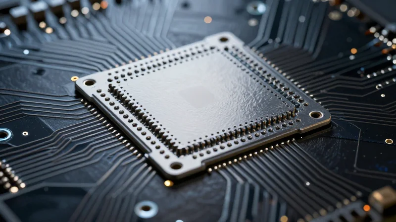
Precision Micro-Via Design Strategies
Micro-vias are the backbone of HDI LiDAR circuitry. To ensure reliability in rigid-flex configurations, designers must prioritize laser-drilled via-in-pad (VIP) configurations. Utilizing stacked or staggered micro-vias requires strict adherence to aspect ratio limits—typically 0.75:1 for copper-filled structures—to prevent barrel cracking during the cyclic thermal stress common in automotive LiDAR environments.
| Parameter | Standard HDI | High-Frequency LiDAR Requirement |
|---|---|---|
| Minimum Micro-via Diameter | 100 µm | 75 µm |
| Aspect Ratio Limit | 1:1 | 0.75:1 |
| Copper Plating Fill | Non-conductive plug | Full copper electrolytic fill |
Trace Width and Spacing Optimization
For high-frequency LiDAR signals, maintaining impedance consistency is paramount. Reducing trace widths to support high density introduces risk in etching uniformity. Designers must employ a 'tapered trace' transition strategy when moving from rigid sections to the flexible polyimide substrate to prevent stress concentration and signal reflection.
- What is the recommended trace-to-copper pour clearance for high-frequency lines?
A minimum of 3x the dielectric thickness is recommended to minimize parasitic capacitance and edge-effect coupling in the high-GHz range. - How does flexible substrate material influence DFM rules?
Polyimide absorption rates require tighter annular ring tolerances to accommodate material shrinkage during multi-layer lamination cycles. - Should I use tented or filled vias?
For high-density LiDAR, fully copper-filled and capped (plated-over) vias are mandatory to ensure planar mounting surfaces and superior signal path integrity.
Material Selection: Coverlay Adhesives and Dielectrics
Adhesive-less vs. Adhesive-based Coverlays
In high-frequency LiDAR applications, the choice between adhesive-based and adhesive-less coverlays significantly dictates signal transmission performance. Adhesive-based systems introduce thicker organic layers with higher dissipation factors, which contribute to signal loss at frequencies above 10 GHz. Conversely, adhesive-less constructions leverage direct copper-to-polyimide bonding, offering superior dimensional stability and a lower dielectric profile, which is essential for maintaining controlled impedance and minimizing insertion loss.
| Feature | Adhesive-based | Adhesive-less |
|---|---|---|
| Dielectric Loss (Df) | Higher | Lower |
| Z-Axis CTE | Less Stable | Highly Stable |
| Signal Integrity | Moderate | Excellent |
| Manufacturing Cost | Budget-friendly | Premium |
Impact of Dielectric Constant (Dk) on High-Speed Signals
The dielectric constant (Dk) of the coverlay and base substrate directly impacts the propagation velocity of signals across the rigid-flex interface. In LiDAR systems, where timing precision is paramount, fluctuations in Dk can result in phase shifts or signal jitter. Engineers must prioritize low-Dk materials (typically in the 2.8 to 3.2 range) to reduce capacitive coupling and prevent parasitic capacitance that degrades signal edges in high-speed digital paths.
Material Selection FAQ
- Why is adhesive-less construction preferred for rigid-flex LiDAR boards?
Adhesive-less materials provide a thinner profile and uniform electrical properties, preventing the signal degradation often caused by the lossy, thicker acrylic adhesives found in standard flexible circuits. - How does moisture absorption affect Dk?
Materials with high moisture absorption rates will see a spike in their Dk value when exposed to ambient humidity, which can lead to unpredictable impedance swings during the field operation of the LiDAR sensor. - What is the primary trade-off when moving to low-Dk materials?
Low-Dk materials are often harder to process during lamination and may require specialized drill bit geometries or plasma desmear cycles to ensure reliable via plating and structural integrity.
Precision Bend Radius Calculations for Flex Zones
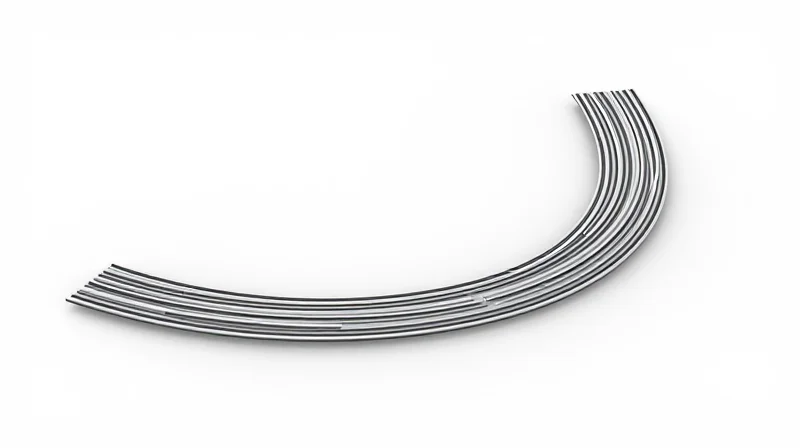
Calculating Minimum Bend Radius for Signal Integrity
For high-frequency LiDAR applications, the minimum bend radius (MBR) is not merely a mechanical constraint but a signal integrity requirement. Excessive stress in the flex zone causes copper elongation, leading to work hardening and micro-cracking that drastically alters impedance profiles. Designers must adhere to the rule of thumb: MBR = 10x to 15x the total thickness of the flex stack-up for dynamic applications, and 6x to 10x for static installation.
| Flex Type | Recommended Multiplier | LiDAR Reliability Impact |
|---|---|---|
| Static (Installation) | 6x - 10x | Low risk of fatigue; protects dielectric bonds. |
| Dynamic (Continuous) | 15x - 20x | Essential for scanning optics movement. |
| High-Frequency RF | 20x+ | Prevents impedance shifts caused by copper deformation. |
Design Guidelines for Stress Mitigation
- Trace Placement
Always route traces perpendicular to the bend axis. Avoid placing copper in the outer radius of the flex zone where tensile stress is highest. - I-Beam Effect Mitigation
Stagger traces on opposite layers to prevent an 'I-beam' effect, which stiffens the flex area and increases the likelihood of trace fracturing. - Neutral Axis Management
Design the circuit stack-up so that the critical high-speed signal layers are centered on the neutral axis of the flex laminate to minimize mechanical strain.
Engineering Verification Checklist
Before finalizing layout, ensure that all high-speed differential pairs passing through flex regions are modeled for mechanical fatigue. LiDAR deployments often involve thermal cycling that exacerbates the brittleness of standard adhesives; therefore, adhesive-less polyimide copper laminates are strongly recommended for tight bend radiuses where frequency stability is paramount.
Controlled Impedance Strategies for High-Frequency Signals

Strategies for Consistent Impedance Profiles
To maintain 50Ω single-ended or 100Ω differential impedance in rigid-flex LiDAR circuits, designers must account for the dramatic dielectric constant (Dk) shifts inherent at the rigid-to-flex interface. The transition zone often experiences geometry discontinuity due to the removal of rigid laminate layers; therefore, ground plane stitching and width compensation are mandatory to mitigate return path discontinuities that degrade signal integrity.
Impedance Management Techniques
| Strategy | Implementation Benefit | Constraint |
|---|---|---|
| Reference Plane Stitching | Maintains continuous return paths through transition zones | Must optimize via spacing to avoid resonant frequencies |
| Copper Weight Adjustment | Compensates for etch factor differences between flex and rigid | Limited by current carrying capacity requirements |
| Localized Reference Planes | Controls fields in unsupported flex areas | Increases risk of mechanical stress at transition edges |
Design Best Practices for LiDAR Interconnects
- How does coverlay impact impedance?
Coverlay adhesives increase the effective Dk of the outer layers. Engineers must simulate impedance with the coverlay in place, as the adhesive flow-out can create localized impedance dips. - Why is differential pair symmetry critical?
Any asymmetry in the rigid-to-flex transition causes common-mode noise, which is fatal for high-frequency LiDAR data transmission. Ensure trace spacing is maintained perfectly even when bending. - What is the role of stitching vias?
Ground stitching vias should be placed within 5-10 mils of the signal transition zone to keep the return current loop area as small as possible, minimizing inductive spikes.
Ultimately, the transition zone requires a simulation-led approach. By utilizing field solvers to model the physical change in stack-up at the transition point, designers can dynamically adjust trace widths to compensate for the absence of rigid core material, ensuring signal performance remains stable across the entire assembly.
Thermal Management in Rigid-Flex Architectures
Managing Heat Dissipation in Rigid-Flex Transitions
Thermal management in LiDAR circuitry is critical, as high-frequency processors and optical emitters generate significant heat that can degrade signal integrity and mechanical flexibility. Unlike standard rigid boards, the flex sections of these assemblies act as thermal bottlenecks because polyimide substrates possess significantly lower thermal conductivity than FR-4 or metal-core alternatives. DFM protocols mandate the integration of copper pours, strategically placed thermal vias, and specialized thermally conductive adhesives to establish continuous thermal bridges across the rigid-to-flex interface.
Comparative Thermal Material Properties
| Material Type | Thermal Conductivity (W/mK) | Application Note |
|---|---|---|
| Polyimide (Flex) | 0.12 - 0.25 | Requires external heat sinks |
| Thermally Conductive Adhesive | 0.80 - 1.50 | Best for interface bridging |
| Copper Foil | 385.00 | Primary thermal conduction path |
| FR-4 (Rigid) | 0.25 - 0.35 | Base board material |
Design Strategies for Thermal Path Optimization
- How can thermal vias be placed without inducing stress in flex zones?
Thermal vias should be concentrated in the rigid sections near the transition zone, using a staggered or hexagonal grid pattern to prevent localized stress risers that could lead to crack propagation in the flex tail. - What is the role of copper thieving in heat management?
Copper thieving, or balanced pour patterns, increases the effective copper surface area, enhancing passive cooling and improving the structural rigidity required to support thermal management components without impacting signal impedance. - Are there limits to using thermal pastes in flex circuits?
Yes, high-modulus thermal interface materials (TIMs) can restrict the bending capability of the flex zone; opt for low-modulus, flexible thermal adhesives that accommodate board movement without delamination.
To prevent mechanical failure, designers must avoid placing thermal vias directly within the dynamic bend radius. Instead, extend thermal planes from the rigid sections into the flex regions using wide, flexible copper fingers. This geometry provides a low-resistance path for heat flux while maintaining the mechanical compliance necessary for robust LiDAR system integration.
Mitigating Manufacturing Defects at the Interface
Root Causes of Interface Delamination
The rigid-flex transition zone is the most mechanically vulnerable point in a LiDAR sensor PCB. Defects often stem from coefficient of thermal expansion (CTE) mismatches between rigid FR-4 and polyimide flex materials, leading to interfacial shear stress during thermal cycling. Proper material selection and transition geometry are critical to preventing delamination.
DFM Strategies for Stack-up Optimization
| Defect Type | Design Mitigation Strategy | Fabrication Adjustment |
|---|---|---|
| Copper Crack/Fatigue | Use I-Beam construction | Eliminate plating in flex area |
| Delamination | Staggered circuit traces | Plasma cleaning pre-lamination |
| Adhesive Bleed-out | Increase coverlay set-back | Optimize pressing temperature |
Common Questions on Interface Reliability
- How can I prevent trace necking at the transition?
Ensure that the transition zone uses a gradual radius for traces rather than sharp 90-degree turns and maintain a minimum distance of 2mm from the rigid-flex interface to the nearest via. - Why should I avoid plating in the flex zones?
Plated-through holes in flexible sections increase material stiffness, drastically reducing the effective fatigue life and increasing the likelihood of barrel cracking under dynamic loads. - Is coverlay or dry film better for high-speed signals?
For high-frequency LiDAR applications, a photo-imageable coverlay (PIC) is generally preferred to maintain tighter tolerance and ensure better dielectric consistency across the high-speed signal path.
Validation and Testing Protocols

Time Domain Reflectometry (TDR) for Impedance Verification
In high-frequency LiDAR applications, even minor impedance discontinuities at the rigid-flex junction can cause significant signal degradation. TDR testing is the industry-standard method for identifying these mismatches. By injecting a fast-rise-time step pulse and analyzing the reflected signal, engineers can map impedance variations along the transmission path with high spatial resolution, allowing for precise design iterations before mass production.
Environmental Stress Testing and Reliability
LiDAR systems operate in harsh automotive environments, necessitating comprehensive stress screening. Validation protocols must address both mechanical fatigue at the flex interface and thermal stability under rapid cycling, ensuring the interconnects maintain electrical integrity throughout the vehicle lifecycle.
| Test Category | Protocol | LiDAR Application Goal |
|---|---|---|
| Signal Integrity | TDR Analysis | Ensure <5% impedance mismatch across interfaces. |
| Thermal Stability | HASS (Highly Accelerated Stress Screening) | Verify bond integrity through 1000+ thermal cycles. |
| Mechanical | Dynamic Flex Testing | Simulate vibration and assembly-induced strain. |
Frequently Asked Questions
- How often should TDR testing be performed?
TDR testing should be conducted as part of the first-article inspection (FAI) and periodically during batch production to ensure material consistency and plating quality at transition vias. - Why is thermal cycling critical for rigid-flex LiDAR boards?
Different coefficients of thermal expansion (CTE) between rigid and flexible substrates can cause delamination or via cracking; stress testing validates that the mechanical interface can withstand these expansion cycles.
Successfully designing for high-frequency LiDAR requires moving beyond standard PCB practices into specialized material and mechanical engineering. By adhering to these DFM best practices, you can ensure your hardware is both high-performing and manufacturable at scale. Contact our engineering team today to review your current board stack-up and identify potential signal integrity optimizations.
