
As automotive sensing requirements push into the 77GHz millimeter-wave spectrum, the margin for error in PCB design has effectively vanished. Designing for high-frequency radar demands more than standard best practices; it requires a deep understanding of physics, material science, and precision manufacturing. In this technical deep-dive, we explore the critical DFM rules that determine whether your radar system succeeds in the field or fails due to signal attenuation and parasitic interference.
Understanding the Challenges of 77GHz Radar Design

The Physics of mmWave Signal Degradation
At 77GHz, electromagnetic wave behavior shifts significantly compared to traditional sub-10GHz PCB designs. The primary challenges originate from the loss tangent of standard substrate materials and the skin effect, which forces current to flow through an increasingly narrow layer of the copper surface.
| Challenge | Physical Mechanism | Impact at 77GHz |
|---|---|---|
| Dielectric Loss | Molecular oscillation energy dissipation | Rapid attenuation of signal amplitude over short traces |
| Skin Effect | Concentration of current at conductor surface | Increased effective resistance and heat dissipation |
| Surface Roughness | Increased path length at microscopic level | Phase jitter and signal integrity degradation |
Managing Frequency-Dependent Losses
To maintain signal integrity, designers must strictly control the PCB stack-up and material properties. The standard FR-4 dielectric is entirely unsuitable for these frequencies, necessitating the use of specialized low-loss laminates with extremely low dissipation factors (Df).
- Why does copper surface roughness matter at 77GHz?
As frequency increases, the skin depth decreases. When the skin depth becomes comparable to the copper surface profile, electrons follow the irregular contours of the copper foil, effectively increasing the path length and electrical resistance. - What role does moisture absorption play?
High-frequency radar signals are sensitive to the dielectric constant (Dk) stability. Moisture absorption in sub-par materials can cause Dk shifts, leading to impedance mismatches and phased array beam steering errors.
Recommendations for Signal Integrity
Designers should prioritize VLP (Very Low Profile) or HVLP (Hyper Very Low Profile) copper foils. By minimizing the peak-to-valley roughness, the resistive losses associated with the skin effect are significantly mitigated, preserving the high-speed signal integrity required for accurate automotive detection.
Substrate Selection: Material Science for mmWave
The Limitations of Conventional Substrates
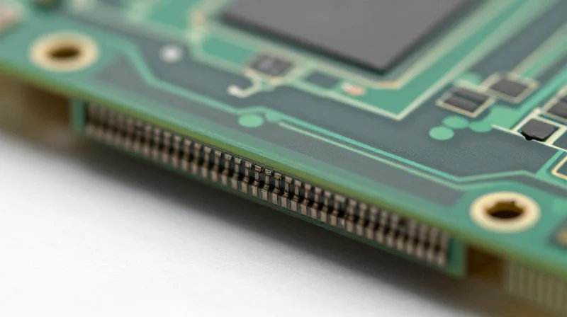
At 77GHz, standard FR-4 substrates suffer from prohibitive dielectric losses and inconsistent glass-weave profiles. The loss tangent (Df) of standard epoxy resins increases thermal instability and signal attenuation to levels that render high-speed automotive radar signals unrecognizable. Furthermore, the heterogeneous nature of glass-reinforced fibers creates localized variations in the dielectric constant (Dk), leading to phase jitter and timing inaccuracies across high-frequency transmission lines.
Comparative Analysis of High-Frequency Materials
| Material Type | Typical Dk (77GHz) | Loss Tangent (Df) | Stability |
|---|---|---|---|
| Standard FR-4 | 4.4 - 4.8 | 0.020 | Poor |
| Modified Epoxy | 3.6 - 3.8 | 0.008 | Moderate |
| PTFE/Ceramic | 2.9 - 3.2 | 0.001 - 0.002 | Excellent |
Key Material Selection Criteria
For 77GHz radar applications, the focus must shift to PTFE-based laminates and ceramic-filled hydrocarbon materials. These substrates provide a tightly controlled Dk, essential for maintaining impedance matching along microstrip and stripline architectures.
- Why is Dk uniformity critical at 77GHz?
The wavelength at 77GHz is extremely short, meaning even minor fluctuations in the dielectric constant due to glass-fiber bundles can cause significant phase errors and reflections. - Does CTE matter for radar modules?
Yes, matching the Coefficient of Thermal Expansion (CTE) between the PCB and the radar chipset ensures long-term solder joint reliability under the harsh automotive thermal cycling environment. - How does surface roughness impact performance?
At mmWave frequencies, the skin effect confines current to a very thin surface layer; therefore, ultra-low-profile copper is mandatory to prevent signal attenuation caused by surface scattering.
Layer Stack-up Optimization for Signal Integrity
Layer Stack-up Optimization for Signal Integrity
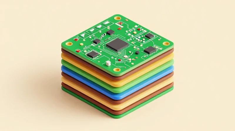
At 77GHz, the PCB stack-up transcends traditional interconnect design, functioning as an integrated microwave waveguide. Achieving signal integrity requires a symmetric, stripline-heavy architecture that maximizes electromagnetic containment. By ensuring each high-speed signal layer is tightly coupled to an adjacent solid reference plane, engineers can effectively suppress parasitic modes and minimize the radiative losses that typically plague mmWave radar modules.
Strategic Plane Configuration
A robust 77GHz stack-up relies on minimizing the distance between the signal trace and the return plane (h-height) to reduce crosstalk while preventing resonance. We recommend a four-to-six layer configuration utilizing ultra-thin core materials to keep the electromagnetic fields tightly confined.
| Parameter | Design Rule for 77GHz | Reasoning |
|---|---|---|
| Dielectric Height | 50-100 micrometers | Reduces dispersion and prevents substrate modes. |
| Plane-to-Plane Gap | Minimal (Symmetric) | Balances internal stresses to prevent board warpage. |
| Via Stitching | 1/10th wavelength | Prevents EMI leakage and cavity resonances. |
Common Implementation Questions
- Why is a symmetric stack-up critical?
Asymmetry induces thermal stresses during the reflow process, leading to board warp, which physically shifts trace impedance and causes phase instability across the phased-array antenna elements. - How does layer spacing affect crosstalk?
Increased distance between signal and ground layers expands the return path current loop; keeping this loop tightly coupled ensures the majority of the magnetic field remains within the dielectric, limiting radiative coupling to adjacent traces. - Should I use buried vias for signal transitions?
Yes, to avoid unnecessary capacitive stubs. At 77GHz, every via stub acts as an antenna; buried or back-drilled vias are mandatory to maintain a continuous transmission environment.
Advanced Impedance Control and Trace Geometry
Precision Geometry at Millimeter-Wave Frequencies
At 77GHz, the signal wavelength is approximately 3.9mm in free space, meaning trace widths and spacings become significant fractions of the wavelength. Even minor manufacturing variations in etching or copper roughness cause drastic fluctuations in characteristic impedance. Designers must move beyond standard PCB manufacturing rules by implementing controlled-depth milling and strictly limiting trace width tolerance to +/- 5% or tighter.
Critical Impedance Factors
| Design Factor | 77GHz Impact | Manufacturing Requirement |
|---|---|---|
| Copper Roughness | Increases resistive loss significantly. | Specify VLP (Very Low Profile) foil. |
| Etch Compensation | Changes trace cross-section geometry. | Use direct imaging for accuracy. |
| Dielectric Thickness | Affects shunt capacitance. | Validate batch-specific Dk/Df. |
Mitigating Parasitic Discontinuities
Discontinuities such as via stubs, pad transitions, and connector interfaces act as primary sources of return loss at 77GHz. To maintain high-speed signal integrity, designers must employ back-drilling to remove residual via stubs and utilize tapered trace transitions when connecting to high-frequency components.
- How does copper roughness affect 77GHz signals?
As frequency increases, current flows primarily on the surface of the conductor due to the skin effect; rough copper profiles introduce scattering and increase effective resistance, leading to insertion loss. - What is the primary goal of trace tapering?
Tapering minimizes impedance mismatch at the transition point between surface mount pads and interconnect traces, preventing signal reflections that degrade the radar performance. - Why is back-drilling mandatory for 77GHz designs?
Residual via barrels act as open-ended stubs that exhibit resonance at high frequencies, creating notches in the frequency response and inducing significant signal attenuation.
Via Design and Grounding Strategies
Minimizing Via-Induced Parasitics at 77GHz
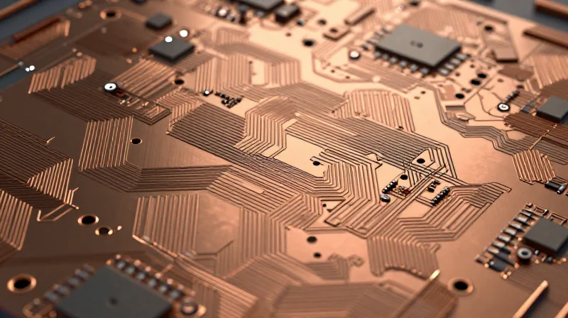
At 77GHz, standard vias act as complex resonant structures that introduce significant inductive and capacitive parasitics. To mitigate these effects, design engineers must minimize the length of the via barrel—the unused portion of the via—which acts as an open-ended stub. Implementing back-drilling or utilizing blind and buried via technologies is mandatory to eliminate these stubs and prevent resonance-driven signal degradation.
| Via Technique | Parasitic Impact | Implementation Suitability |
|---|---|---|
| Through-hole | High (Stub effect) | Not recommended |
| Back-drilling | Low | High (Cost-effective) |
| Blind/Buried | Minimal | High (Premium performance) |
Ground Return Path and Via Stitching
Maintaining a continuous, low-impedance ground return path is the cornerstone of radar module reliability. When signal traces transition between layers, the accompanying ground return current must follow the trace closely to minimize loop area. Placing ground stitching vias in immediate proximity to signal transition vias is critical to providing a continuous path for return currents, thereby reducing radiated EMI and preventing signal reflections caused by impedance discontinuities.
- What is the optimal spacing for ground stitching vias?
Stitching vias should be placed no further than 1/10th of a wavelength of the operating frequency from the signal via to ensure a stable return path and effective suppression of cavity resonances. - How does anti-pad design affect 77GHz performance?
Anti-pads must be carefully sized to control the parasitic capacitance of the via transition; failing to optimize these clearances creates localized impedance dips that result in signal reflections. - Should thermal relief be used on ground vias?
Thermal relief patterns must be avoided on RF ground connections as they introduce excessive inductance; all ground vias should feature a direct, solid connection to the ground planes.
DFM Rules for High-Density Interconnect (HDI)
HDI Design Guidelines for mmWave Reliability
Implementing HDI in 77GHz radar modules requires balancing high integration density with the stringent electromagnetic requirements of mmWave signals. At these frequencies, HDI transitions—specifically micro-vias and blind via structures—must be meticulously engineered to prevent impedance discontinuities and signal leakage.
Critical DFM Constraints for HDI
| Feature | Recommended DFM Constraint | Radar Impact |
|---|---|---|
| Micro-via Aspect Ratio | Maximum 0.75:1 | Ensures reliable copper plating to prevent open circuits |
| Via Capture Pad | Minimum 100µm over drill | Maintains structural integrity during thermal cycling |
| Copper Plating Thickness | Minimum 15µm in via barrel | Reduces resistive losses and parasitic inductance |
| Dielectric Separation | Minimum 50µm between layers | Mitigates inter-layer crosstalk and dielectric breakdown |
FAQs on HDI Integration
- How do I mitigate via-induced reflections in HDI?
Utilize laser-drilled blind vias to minimize the stub length. Excess via stubs act as antennas at 77GHz, causing significant return loss and resonance issues. - Why is copper plating uniformity critical for radar?
Uneven plating creates variations in characteristic impedance. In high-speed automotive radar, even minor localized impedance shifts can lead to signal degradation and poor phase consistency. - Are stacked vias recommended for 77GHz designs?
Avoid stacking vias if possible; staggered micro-vias are preferred to prevent structural weakness and reduce the surface area that could contribute to impedance mismatch.
Manufacturing Tolerances and Thermal Management
Precision Manufacturing and CTE Management
At 77GHz, the wavelength of the signal is extremely short, making mechanical tolerances and material stability paramount. Even minor deviations in dielectric constant or trace geometry—often caused by thermal expansion—can shift the resonant frequency of radar antennas and degrade performance. Designers must prioritize substrates with low Coefficient of Thermal Expansion (CTE) to ensure that the PCB maintains structural integrity across the harsh operating temperatures of an automotive engine environment, which can range from -40°C to +125°C.
| Parameter | Tolerance Constraint | Impact on 77GHz Performance |
|---|---|---|
| Trace Width | +/- 5% or 0.5 mil | Impedance mismatch and signal reflection |
| Dielectric Thickness | +/- 3% | Phase velocity variance and antenna squint |
| Registration | < 1 mil | Via-to-pad misalignment and radiation leakage |
Thermal Management Strategies
Heat dissipation in high-power automotive radar modules is a significant challenge due to the high density of MMIC (Monolithic Microwave Integrated Circuit) components. Excessive heat leads to increased resistive losses and dielectric breakdown. Effective thermal management involves utilizing high-thermal-conductivity laminates, integrated copper coins, and thermal vias that connect the MMIC ground pad to the bottom-side heat sink.
- How does CTE mismatch affect radar reliability?
CTE mismatch between the PCB substrate and the copper features can lead to micro-cracking in vias and solder joints during thermal cycling, eventually resulting in open circuits or intermittent signal degradation. - Why is copper plating thickness critical for 77GHz?
Uniform copper plating ensures consistent impedance across the board. Variability in plating thickness can lead to 'skin effect' losses, which are significantly amplified at mmWave frequencies, causing substantial signal attenuation. - What role do thermal vias play in signal integrity?
Beyond heat dissipation, thermal vias must be carefully placed to avoid creating ground bounce or impedance discontinuities in the signal return path, necessitating a balanced design between thermal efficiency and RF performance.
Verification and Simulation Techniques

The Role of 3D Electromagnetic Field Solvers
At 77GHz, standard 2D transmission line models are insufficient because they fail to account for complex 3D parasitic effects such as via stubs, solder ball transitions, and non-ideal material dispersion. Designers must employ full-wave 3D electromagnetic (EM) field solvers—such as Ansys HFSS or CST Studio Suite—to accurately predict S-parameters, insertion loss, and phase stability across the mmWave spectrum.
Critical Verification Workflows
- Pre-Layout Extraction
Utilizing stack-up analysis to verify dielectric constants (Dk) and dissipation factors (Df) under simulated thermal stress before routing begins. - Post-Layout EM Validation
Exporting GDSII or ODB++ design files to extract exact physical geometries, ensuring that manufacturing tolerances, such as etch-back and copper roughness, are included in the simulation model. - Multiphysics Co-Simulation
Integrating electrical, thermal, and mechanical solvers to evaluate how CTE mismatches during reflow alter high-frequency impedance, preventing failures in radar sensing accuracy.
Simulation vs. Reality: Comparison of Approaches
| Methodology | Accuracy at 77GHz | Computational Cost | Primary Use Case |
|---|---|---|---|
| 2D/2.5D Field Solver | Low | Low | Initial routing feasibility |
| Full-Wave 3D EM Solver | Very High | High | Final sign-off for critical mmWave paths |
| Multiphysics Modeling | High | Very High | Reliability and thermal sensitivity analysis |
Best Practices for Simulation Accuracy
To ensure simulation correlates with prototype measurement, engineers should always apply a 'sensitivity analysis' to key manufacturing variables. Specifically, vary the substrate dielectric constant by ±0.05 and copper thickness by ±0.5 mils in the simulation suite to see how these expected fabrication variations affect antenna gain and side-lobe levels.
Achieving peak accuracy in 77GHz radar systems is a rigorous process that bridges the gap between theoretical RF design and real-world manufacturing constraints. By adhering to these advanced DFM guidelines and focusing on material integrity, you can ensure your automotive sensing solutions meet the highest standards of safety and performance. Contact our engineering team today to review your current radar PCB layout and optimize your design for manufacturing success.
