
In the fast-paced world of autonomous vehicle development, every decibel of signal integrity and every fraction of production waste directly impacts the bottom line. As Tier 1 suppliers race to deliver next-generation ADAS radar units, the choice of high-frequency materials and board architecture has evolved from a technical detail into a critical strategic advantage.
The High-Frequency Challenge in ADAS Radar Systems

As ADAS radar systems shift toward the 77-81 GHz range to support higher resolution, the physics of signal propagation become significantly more punishing. At these millimeter-wave frequencies, the margin for error in PCB design vanishes, forcing engineers to reconcile raw electromagnetic performance with the realities of high-volume manufacturing costs.
Core Engineering Hurdles
- Signal Attenuation
As frequency increases, dielectric loss and conductor surface roughness cause exponential increases in signal loss, directly reducing the maximum detection range of the radar sensor. - Interference and Crosstalk
At 77 GHz, wavelength dimensions are microscopic, making trace geometry and substrate homogeneity critical to preventing unwanted coupling and electromagnetic interference that corrupt target detection. - Thermal Management
High-frequency materials often possess lower thermal conductivity, necessitating advanced heat dissipation strategies to prevent signal frequency drift and premature component failure.
Impact of Material Properties on Radar Performance
| Parameter | Effect on Radar | Design Implication |
|---|---|---|
| Dielectric Constant (Dk) Stability | Phase velocity variation | Tight tolerance requirements |
| Dissipation Factor (Df) | Signal attenuation (insertion loss) | Requires PTFE or ceramic-filled laminates |
| Copper Foil Roughness | Skin effect losses | Use of VLP (Very Low Profile) copper |
The Cost-Performance Trade-off
Maximizing ROI requires selecting materials that meet the strict electrical requirements for 77 GHz operation without over-engineering for features that do not improve functional safety. High-performance laminates—often using specialized resin systems—are costly; therefore, optimizing stack-up configurations to reduce the usage of high-loss materials in non-critical layers is essential for keeping manufacturing costs viable for mass-market deployment.
Strategic Material Selection: Beyond Standard FR-4
The Limitations of Conventional FR-4 in Autonomous Applications
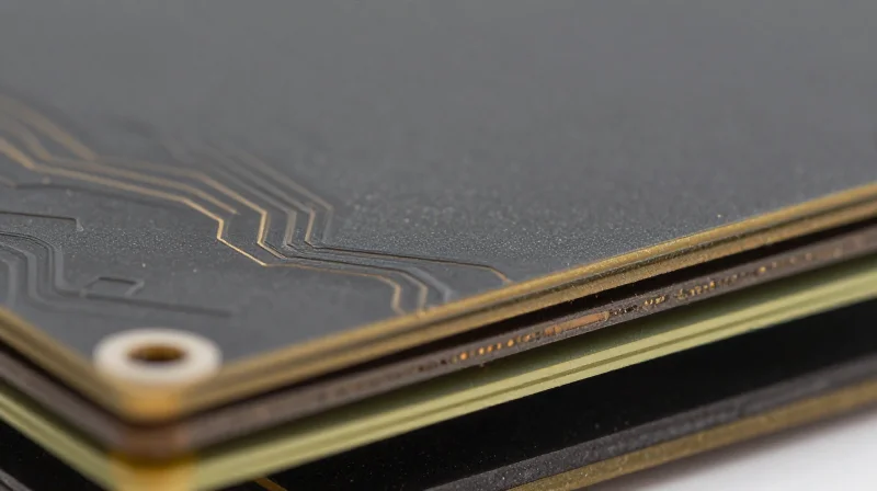
While FR-4 is the industry standard for consumer electronics, its high dissipation factor (Df) and unstable dielectric constant (Dk) over frequency make it unsuitable for 77 GHz-81 GHz radar sensors. As autonomous vehicles rely on high-precision object detection, signal loss inherent in FR-4 laminates results in decreased range, increased noise, and severe thermal management issues, directly compromising the ROI of the vehicle's sensor suite.
Comparative Performance Analysis of Advanced Substrates
| Material Type | Dielectric Constant (Dk) | Dissipation Factor (Df) | Thermal Stability |
|---|---|---|---|
| Standard FR-4 | 4.4 - 4.8 | 0.020 | Low |
| High-Tg Epoxy | 3.8 - 4.2 | 0.015 | Moderate |
| PTFE-based Laminate | 2.1 - 3.0 | 0.001 - 0.002 | Excellent |
| Ceramic-filled Hydrocarbon | 3.0 - 3.5 | 0.003 - 0.004 | High |
Strategic Advantages of PTFE and Specialized Laminates
For autonomous vehicle radar, PTFE-based substrates provide the industry's lowest dielectric loss. These materials minimize phase distortion and ensure signal phase consistency—factors that are vital for Beamforming and Frequency Modulated Continuous Wave (FMCW) radar operations. By investing in these high-performance materials early in the development cycle, engineers prevent costly redesigns necessitated by signal integrity failures in the field.
Frequently Asked Questions Regarding Advanced Materials
- Why is the Dissipation Factor (Df) the most important metric?
Df represents the energy lost as heat within the material. In millimeter-wave radar, a high Df leads to significant signal attenuation, effectively shortening the radar's detection range. - Can hybrid PCB designs provide a cost-effective middle ground?
Yes. Hybrid designs allow for expensive high-frequency laminates to be used only in the RF signal path, while standard materials are used for the supporting control layers, effectively balancing performance with manufacturing costs. - How does moisture absorption affect material choice?
Autonomous vehicles operate in diverse environments. Materials with low moisture absorption are essential to prevent the dielectric constant from shifting, which would otherwise cause radar frequency drift.
Minimizing Signal Loss through Advanced PCB Topology
Optimizing Signal Paths for Millimeter-Wave Performance
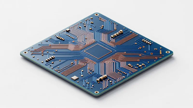
To minimize signal loss in high-frequency autonomous vehicle applications, engineers must move beyond basic routing to prioritize precise trace geometry, via transition management, and strict impedance control. At frequencies exceeding 77GHz, parasitic effects—which are often negligible in standard consumer electronics—become primary sources of attenuation and crosstalk. Minimizing these losses requires a holistic approach to the physical layer, ensuring that the transition from chip to antenna is as transparent to the signal as possible.
Critical Topology Considerations
- Controlled Impedance Vias
Utilize back-drilling to remove unused via stubs, which act as resonant antennas at millimeter-wave frequencies, causing significant signal reflection and energy loss. - Differential Pair Coupling
Maintain precise symmetry in differential trace routing to prevent common-mode noise and mode conversion, which degrade the signal-to-noise ratio in critical sensor feedback loops. - Substrate-Integrated Waveguides (SIW)
Implement SIW structures within the PCB layers to confine electromagnetic energy effectively, significantly reducing radiation leakage compared to traditional microstrip lines.
Impact of Topology on Signal Integrity
| Design Technique | Primary Benefit | ROI Impact |
|---|---|---|
| Back-drilling | Reduced reflection | High signal fidelity |
| SIW Integration | Lower insertion loss | Extended sensing range |
| Tight Pitch Via Fencing | Reduced EMI/Crosstalk | Improved system reliability |
The focus on advanced topology is not merely an engineering preference but a financial necessity for ROI. By investing in optimized trace geometry early in the design cycle, companies can significantly reduce the number of prototyping iterations required to meet stringent automotive compliance standards. When signal loss is mitigated at the PCB level, the reliance on high-cost, high-power signal boosters or error-correction software is lowered, streamlining the overall BOM cost and extending the operational lifecycle of the autonomous vehicle's sensory suite.
Impact of Manufacturing Precision on Production Yields
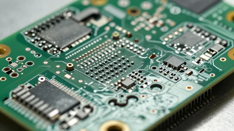
In the production of high-frequency radar sensors for autonomous vehicles, manufacturing precision serves as the primary lever for controlling yield. When operating at millimeter-wave frequencies, the margin for error is measured in microns. Any deviation in physical dimensions—be it drill wander, plating thickness uniformity, or etching undercut—shifts the electromagnetic behavior of the PCB, resulting in failed performance tests and costly scrap. By implementing stringent process controls, manufacturers can significantly reduce the 'hidden costs' associated with rework and final-stage assembly rejection.
Critical Process Parameters and Their Yield Impact
| Process Variable | Common Failure Mode | Impact on Yield |
|---|---|---|
| Drill Registration | Pad breakout/Stub formation | High signal reflection |
| Copper Plating | Barrel cracking/Thin walls | Intermittent connectivity |
| Etch Control | Over-etching/Trace width loss | Impedance mismatch |
Strategies for Enhancing Process Repeatability
To stabilize production yields, manufacturers must move beyond standard fabrication tolerances. This includes the adoption of laser-direct drilling for via precision, which eliminates the mechanical stress of traditional bits, and the use of modified semi-additive processes (mSAP) for ultra-fine trace definition. By optimizing the metal-to-dielectric ratio during etching, developers can ensure that impedance remains consistent across the entire panel, minimizing variations that lead to localized signal degradation.
- How does etching precision affect radar performance?
Precision etching ensures that trace widths remain within narrow impedance tolerances; even a 5% deviation can cause phase shifts that degrade target detection accuracy in radar sensors. - Can better plating techniques save material costs?
Yes, by utilizing uniform electrolytic deposition, you reduce the need for 'oversized' designs or additional grounding layers, optimizing material usage while improving signal reliability. - What is the role of automated optical inspection (AOI)?
AOI acts as a critical quality gate, allowing manufacturers to identify defects at the inner-layer stage before expensive lamination, effectively salvaging potential scrap.
Lowering Total Cost of Ownership (TCO) via Smart Engineering
Strategic Cost Reduction Through Design Optimization
Reducing the TCO in high-frequency automotive radar modules is achieved by minimizing the 'hidden costs' of manufacturing—specifically high scrap rates and premature field failures. By prioritizing signal integrity at the initial design phase, manufacturers can avoid the costly iterative redesign cycles that often plague autonomous vehicle sensor development. Smart engineering integrates high-performance materials with manufacturing constraints early, ensuring that production remains scalable without compromising the electrical performance required for safety-critical radar systems.
| Cost Driver | Reactive Approach (High TCO) | Proactive Smart Engineering (Low TCO) |
|---|---|---|
| Material Selection | Overspecifying expensive low-loss laminates | Balanced stack-up using hybrid substrates |
| Yield Management | Rework and troubleshooting post-assembly | Automated DFM analysis and precision tooling |
| Product Longevity | Field failures due to thermal cycling | CTE-matched materials for long-term durability |
Optimizing Life-Cycle Value
The transition to smart engineering dictates that PCB design must account for environmental stressors common in automotive applications, such as extreme thermal fluctuations. Leveraging materials with controlled coefficients of thermal expansion (CTE) reduces mechanical strain on solder joints, significantly lowering warranty claims and field maintenance costs. Furthermore, implementing advanced impedance control early in the design cycle allows for tighter manufacturing tolerances, which prevents signal loss issues from emerging only after the boards reach the mass production floor.
- How does early material selection impact TCO?
Choosing the correct dielectric constant (Dk) and loss tangent (Df) at the start prevents the need for excessive shielding or complex corrective board logic, saving both unit cost and assembly time. - Can DFM (Design for Manufacturing) significantly reduce waste?
Yes, by aligning PCB dimensions with standard panel sizes and optimizing etch compensation, manufacturers can maximize material utilization and reduce raw material scrap rates by up to 20%. - Does higher initial investment in design lower TCO?
Absolutely; investing in comprehensive signal integrity simulations and rigorous design reviews prevents catastrophic failures that are exponentially more expensive to fix during the vehicle integration stage.
Accelerating Time-to-Market for Tier 1 Suppliers

Strategic Integration of Simulation and Rapid Prototyping
Tier 1 suppliers face intense pressure to deliver high-performance radar and LiDAR PCBs under aggressive development timelines. By shifting focus toward virtual prototyping and simulation-driven design, engineers can validate electromagnetic performance and signal integrity long before physical prototypes are manufactured. This front-loading of validation minimizes the 'test-fail-redesign' loop, effectively collapsing the product development lifecycle.
| Strategy | Impact on Speed | Benefit to ROI |
|---|---|---|
| Virtual Prototyping | High | Reduces material waste |
| Additive PCB Manufacturing | Medium | Fast iteration cycles |
| Digital Twin Implementation | High | Predicts manufacturing yield |
Streamlining the Transition to Volume Production
Rapid scaling depends on design for manufacturing (DFM) protocols that account for high-frequency material constraints early in the layout phase. Aligning material selection—such as specialized PTFE or ceramic-filled laminates—with scalable manufacturing capabilities ensures that high-performance designs do not require expensive re-engineering when transitioning from prototype to high-volume production.
- How does early material selection affect scaling?
Selecting stable, mass-producible high-frequency materials prevents the need for redesigning stackups when moving from low-volume pilot runs to high-volume production. - Can simulation tools replace physical testing?
While they cannot entirely replace final compliance testing, they drastically reduce the number of physical iterations required to pass automotive certification standards. - What is the primary driver of delays in Tier 1 PCB development?
The primary driver is iterative debugging caused by failing signal integrity or thermal management requirements discovered late in the testing phase.
Future-Proofing Radar Platforms for Next-Gen Autonomy
The Shift Toward 4D Imaging and High-Resolution Radar
As autonomous vehicles demand granular spatial awareness, legacy radar designs are reaching their limits. Future-proofing necessitates a pivot toward 4D imaging radar, which requires significantly higher bandwidth and lower signal insertion loss. To remain competitive, engineers must prioritize high-frequency, low-loss laminates that maintain thermal stability under high-density component loads.
| Parameter | Legacy Radar | Next-Gen 4D Imaging |
|---|---|---|
| Frequency Band | 24 GHz / 77 GHz | 77-81 GHz / E-Band |
| Dielectric Constant (Dk) | Standard (>3.5) | Low (<3.0, stable) |
| Thermal Management | Standard Heat Sinks | Advanced Thermal Via Arrays |
Strategic Material Selection for Longevity
The selection of PTFE-based or hydrocarbon-ceramic hybrid laminates is critical for maintaining signal integrity over the operational lifespan of the vehicle. These materials provide the necessary dielectric consistency required to prevent 'radar drift,' ensuring that performance remains stable despite extreme temperature fluctuations typical in automotive environments.
Frequently Asked Questions on Radar Autonomy
- How do we balance cost with performance in radar PCB design?
Utilize hybrid material stacks, placing high-performance laminates only in the high-frequency RF sections while using cost-effective FR4 materials for control circuitry layers. - Will 4D radar require a complete overhaul of current manufacturing lines?
Most existing lines can be adapted through upgraded laser-direct-structuring (LDS) or refined etching processes, provided the design incorporates tighter tolerances from the prototyping phase. - What role does signal integrity simulation play in future-proofing?
Predictive modeling allows engineers to account for manufacturing variations in copper roughness and resin content, preventing costly post-production failures before full-scale deployment.
Optimizing high-frequency PCB manufacturing is no longer just about meeting technical specifications; it is about building a scalable foundation for competitive advantage in the automotive sector. By prioritizing material integrity and manufacturing precision, Tier 1 suppliers can significantly reduce waste and accelerate development timelines. Contact our engineering team today to discuss how we can optimize your next ADAS radar design for superior performance and cost efficiency.
