
Designing for the 'pet-proof' environment is one of the most grueling challenges in hardware engineering. When your PCB must withstand constant moisture, physical impacts, and the relentless curiosity of a pet, standard design rules fail. This guide breaks down the mission-critical DFM strategies required to pack GPS performance into a miniaturized, waterproof, and ruggedized footprint.
The Triple Constraint: Size, Sealing, and Signal Integrity

The Engineering Conflict: Miniaturization vs. Environmental Protection
The primary challenge in modern ruggedized GPS design lies in the intersection of density and physics. Achieving an IP67 or IP68 rating requires robust mechanical housing, O-rings, and compression points that consume significant PCB real estate. As engineers push for smaller form factors, the reduction in available space forces a direct trade-off between the integrity of the environmental seal and the performance of the GPS antenna.
Comparative Impact of Design Constraints
| Design Constraint | Miniaturization Strategy | Impact on Ruggedization |
|---|---|---|
| Component Placement | High-density SMT | Increased risk of mechanical stress fractures |
| Housing Clearance | Thin-wall molding | Reduced structural rigidity for O-ring sealing |
| Antenna Proximity | Integration near metal shells | Severe signal attenuation and detuning |
Signal Integrity in Constrained Environments
Maintaining GPS signal integrity within a sealed, compact enclosure is complex because the protective layers often introduce electromagnetic interference (EMI) or signal path loss. Conductive gaskets used for sealing can act as noise traps if not properly grounded, while proximity to compact internal battery arrays often introduces unwanted switching noise into the RF front-end.
- How does PCB thickness influence waterproof sealing?
Thinner PCBs are prone to flexing under the mechanical pressure of O-ring compression, which can lead to hairline cracks in solder joints or micro-fractures in the housing seal. - Why is antenna tuning difficult in miniaturized modules?
Miniaturization forces the antenna closer to the module casing; if the casing is metallic or coated with shielding materials, it creates frequency detuning that is difficult to calibrate in the field. - What is the primary risk of high-density component placement?
High component density reduces the 'keep-out' zones required for RF decoupling, leading to increased crosstalk and susceptibility to interference from the device's internal power management systems.
Substrate Selection for Humid Environments
Mitigating Delamination through Material Selection
In compact, ruggedized GPS modules, standard FR4 often fails when subjected to the thermal cycling and moisture ingress characteristic of humid environments. To prevent catastrophic PCB delamination and trace oxidation, designers must prioritize substrates with high Glass Transition Temperatures (Tg) and low Moisture Absorption coefficients. High-Tg FR4 (typically >170°C) is the baseline requirement, but for extreme applications, moving toward specialized laminates like polyphenylene ether (PPE) or polyimide becomes necessary to ensure mechanical stability and prevent dielectric constant (Dk) drift caused by water molecules infiltrating the board structure.
Substrate Material Comparison for Humid Conditions
| Material Type | Tg Value | Moisture Absorption | Recommended Use |
|---|---|---|---|
| Standard FR4 | 130-140°C | 0.20% - 0.50% | General consumer indoor use |
| High-Tg FR4 | 170-180°C | 0.10% - 0.20% | Ruggedized GPS modules |
| Polyimide | >250°C | 0.05% - 0.10% | High-reliability, aerospace, extreme humidity |
Key Design Considerations for Humidity Resistance
- How does moisture impact signal integrity?
Water absorption in the substrate increases the dielectric constant (Dk) and dissipation factor (Df), resulting in signal attenuation and center-frequency shifting for sensitive GPS RF chains. - Why is the moisture absorption rate the primary DFM metric?
Low moisture absorption prevents the internal expansion that leads to inter-layer delamination, which is the leading cause of field-failure in hermetically sealed but moisture-exposed electronics. - Should I consider metal-core PCBs?
Metal-core substrates provide superior thermal dissipation and stiffness; however, they require careful edge-sealing design to prevent galvanic corrosion between the core and copper layers when exposed to moisture.
Mastering High-Density Interconnect (HDI) Layout Rules
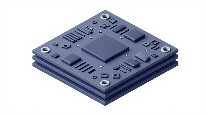
Navigating HDI Design Constraints
Achieving high density in GPS modules requires a shift from standard PCB design to rigorous HDI (High-Density Interconnect) methodologies. In space-constrained waterproof enclosures, managing thermal dissipation and layer-to-layer registration is paramount to prevent moisture-induced failure at micro-via sites.
Via-in-Pad and Micro-via Strategy
For GPS modules, implementing via-in-pad plated over (VIPPO) is necessary to save space, but it introduces specific DFM risks. Always specify non-conductive epoxy filling and copper capping to prevent solder wicking and potential voiding, which can become moisture traps under environmental stress.
| Via Type | Typical Diameter | Best Application |
|---|---|---|
| Laser Micro-via | 0.1mm - 0.15mm | High-density signal routing in BGA escapes |
| Blind/Buried Via | 0.2mm - 0.25mm | Inter-layer signal transition without surface real estate |
| Through-Hole | 0.3mm+ | Power/Ground planes and structural reinforcement |
Trace Width and Impedance Control
GPS signal paths, particularly from the antenna to the LNA, require strictly controlled 50-ohm impedance. In compact boards, use thinner traces (3-mil) with calculated dielectric spacing to minimize parasitic capacitance that could shift the resonant frequency of the antenna.
Common HDI Layout Questions
- How do blind vias affect waterproof integrity?
Blind vias are preferred as they do not penetrate the outer layers of the PCB, reducing the number of surface entry points for moisture and simplifying gasket sealing requirements. - What is the minimum trace-to-via clearance?
For robust manufacturing, maintain a minimum of 4 mils of clearance to prevent bridge shorts during the electrolytic plating process in high-density areas. - Are buried vias recommended for GPS signals?
Yes, buried vias help minimize EMI interference by keeping high-frequency GPS signals on inner layers, shielded by external ground planes.
Strategic Component Placement for Thermal and Impact Resistance

Component Zoning for Mechanical Resilience
In compact, ruggedized GPS modules, the PCB acts as both an electrical carrier and a structural member. To prevent solder joint fatigue and micro-cracking caused by shock and vibration, active components must be placed outside the 'flex zones' of the enclosure. Avoid placing heavy components like TCXOs or large tantalum capacitors near mounting holes or connectors, which serve as mechanical stress concentrations. By maintaining a 5mm keep-out zone from structural fasteners, you significantly improve the fatigue life of fragile GPS RF circuits.
Thermal Management vs. Waterproofing
Ruggedized modules often rely on sealed, low-airflow enclosures, which trap heat generated by the GNSS receiver and auxiliary processing units. Thermal vias and copper pours act as the primary heat sinks. However, in waterproof designs, you must ensure that these copper heat-spreader planes do not bridge to the enclosure's potential thermal expansion points, which could lead to case deformation. Utilize thermally conductive, non-corrosive gap fillers to interface between the PCB's thermal relief zones and the inner housing wall.
| Component Type | Placement Priority | Reasoning |
|---|---|---|
| GPS Chipset/RF IC | Centralized | Minimize trace length and interference. |
| Mounting Holes | Isolation | Prevent mechanical torque transfer to solder joints. |
| TCXO | Thermal Shielded | Protect frequency stability from rapid temperature shifts. |
| Connectors | Peripheral | Must reside at enclosure seal interfaces. |
Frequently Asked Questions on Strategic Layout
- How do I protect the GPS antenna from chassis vibration?
Use a flexible adhesive or mechanical damper between the antenna housing and the PCB, and ensure the RF signal line utilizes a soft-solder or spring-contact connection to decouple vibrational energy from the main board. - Can I use the entire PCB ground plane for heat dissipation?
No, because the ground plane often needs to be segmented to prevent RF noise coupling; use thermal islands connected via thermal vias to effectively move heat while maintaining signal integrity. - Is board thickness critical for impact resistance?
Yes, a thicker PCB reduces board flex, but it increases weight. For ruggedized applications, a 1.2mm or 1.6mm board is standard, provided the enclosure supports the board evenly across its entire surface area.
Advanced PCB Conformal Coating Strategies
Achieving an IP67 or IP68 rating in high-density GPS modules requires more than a simple resin dip. Advanced DFM requires a strategic approach to coating chemistry—balancing moisture vapor transmission rates (MVTR) with secondary operations like connector masking. Improper application in tight form factors often leads to 'wicking' into sensitive micro-connectors, causing signal attenuation and mechanical failure.
Silicone vs. Parylene: Material Selection Matrix
| Attribute | Silicone | Parylene |
|---|---|---|
| Application Method | Spray/Brush/Dip | Vapor Deposition |
| Dielectric Strength | High | Superior |
| Film Uniformity | Low (Edge pooling) | High (Uniform thickness) |
| Reworkability | Moderate | Difficult |
| Thermal Stability | Excellent | Good |
Advanced Masking and Keep-Out Zone Strategies
To prevent coating migration into board-to-board connectors or antenna pads, implement 'dams' or 'moats' during the PCB layout phase. By etching a 0.5mm clear-mask channel around high-risk interfaces, you provide a mechanical barrier that prevents capillary action from pulling low-viscosity coatings into critical electrical contact points.
Frequently Asked Questions on Coating Integration
- How do I prevent Parylene from entering connector housings?
Utilize precision-machined mechanical masks or peelable latex-based solder masks applied prior to vapor deposition. Ensure the mask geometry accounts for a 50-micron tolerance to prevent vapor seepage. - Does conformal coating affect GPS antenna gain?
Yes, high-dielectric coatings shift the resonant frequency of patch antennas. DFM rules must include a 'clear-zone' on the antenna radiating surface or adjust the antenna matching network to compensate for the dielectric constant of the chosen coating. - What is the best way to inspect for coating voids?
Incorporate UV-fluorescent tracers into the coating formulation. Automated Optical Inspection (AOI) systems using UV light can detect pinhole voids or improper edge coverage in seconds.
Antenna Tuning in Micro-Enclosures

Managing Near-Field Detuning in Waterproof Enclosures
Waterproof enclosures introduce a significant dielectric constant variation when the exterior surface is wet, shifting the antenna's resonant frequency. To combat this, design engineers must employ frequency-offset tuning strategies where the antenna is pre-tuned slightly higher than the L1 GPS center frequency (1575.42 MHz), allowing the added capacitance of water film or radome contact to pull the center frequency back into the target band.
Material Impact on Resonant Frequency
| Material Environment | Dielectric Constant (Dk) | Frequency Shift Direction |
|---|---|---|
| Dry Air (Baseline) | 1.0 | None |
| Water Film (Wet) | 80.0 | Downshift (Major) |
| Polycarbonate Radome | 2.9 - 3.2 | Downshift (Minor) |
| Conductive/Metal Housing | N/A (Eddy Currents) | Impedance Mismatch |
Best Practices for Enclosure Integration
- How does enclosure proximity affect gain?
Conductive housing walls near the antenna perimeter excite surface currents, causing pattern distortion and reduced gain; maintain a clearance of at least 0.15 wavelengths from the antenna radiating edge to any metal surface. - Why prioritize radome distance?
The distance between the antenna top surface and the interior face of the waterproof cover should be maximized; keeping a minimum air gap of 1.5mm minimizes the dielectric loading effect of the housing material itself. - Is active tuning necessary for compact modules?
For ultra-compact form factors, passive matching network adjustments are often insufficient; consider utilizing wideband ceramic chip antennas that exhibit a stable VSWR across the required operational spectrum even when detuned.
Implementation Workflow
# Optimization Script Logic for Antenna Tuning
if enclosure_material == 'conductive':
    apply_keepout_zone(radius=0.15 * wavelength)
    adjust_matching_network(pre_shift_freq_offset=+15MHz)
else:
    apply_radome_compensation(material_dk=3.0, gap_min=1.5mm)
    verify_vswr_under_water_load()
DFM for Automated Assembly and Inspection
Optimizing Automated Assembly for Ruggedized GPS Modules
To achieve high-yield assembly of compact, waterproof GPS modules, design for automated manufacturing (DFM) must prioritize pick-and-place stability and solder joint reliability. By incorporating standardized fiducials and utilizing machine-vision-friendly land patterns, manufacturers can significantly reduce alignment errors common in small-scale, high-density PCBs.
Critical DFM Parameters for Automated Throughput
| Design Rule | Recommended Practice | Impact on Assembly |
|---|---|---|
| Fiducial Placement | 3 fiducials per side; 1.0mm min clearance | Enhances SMT machine vision alignment |
| Component Pitch | Maintain >0.5mm for fine-pitch parts | Reduces solder bridging risks |
| Solder Mask | Defined pads with webbed dams | Prevents shorts during reflow |
Automated Inspection Strategies for Waterproofing
Post-assembly inspection must verify not only electrical functionality but also the integrity of sealing surfaces. Automated Optical Inspection (AOI) should be calibrated to detect micro-voids in conformal coating or debris that could compromise the O-ring seals critical for the module's waterproof rating.
- How can I improve AOI effectiveness for conformal coating?
Utilize UV-fluorescent dyes within the conformal coating material to ensure automated systems can easily verify 100% coverage across complex board geometries. - What is the role of In-Circuit Testing (ICT) in GPS modules?
ICT verifies power rails and antenna matching circuit continuity, ensuring that component assembly hasn't shifted resonant frequencies before the enclosure is sealed.
import cv2
# Example pseudo-script for automated visual check of O-ring groove
def verify_seal_clearance(image_path):
    image = cv2.imread(image_path)
    # Detect potential debris within the gasket boundary
    debris = detect_anomalies(image, threshold=0.05)
    return len(debris) == 0
Testing Protocols for Long-Term Field Reliability
Validating Endurance: HALT and HASS Protocols
Highly Accelerated Life Testing (HALT) and Highly Accelerated Stress Screening (HASS) are mandatory for pet-worn GPS devices. Unlike standard consumer electronics, these units face unpredictable mechanical shocks from running, collisions, and constant vibration. We utilize HALT during the design phase to force early failures in solder joints and enclosure seals, while HASS ensures that production batches meet the established reliability threshold.
| Stress Factor | HALT Goal | HASS Implementation |
|---|---|---|
| Thermal Cycling | Identify PCB delamination | Verify production solder integrity |
| Vibration/Shock | Detect component fatigue | Confirm mechanical fixation |
| Moisture/Pressure | Test seal degradation rate | Verify hermetic enclosure integrity |
Pressure Testing and Waterproofing Verification
Water ingress is the primary failure mode for miniaturized tracking hardware. Beyond standard IPX7 rating tests, engineers must perform vacuum decay and pressure chamber testing to mimic the water pressure encountered when a pet swims. Implementing a 'pre-assembly' air-leak test on empty enclosures is a key DFM rule that prevents wasting expensive PCBA components on housings with hairline mold defects.
Reliability FAQ
- How do you test seal degradation over time?
Perform accelerated aging by exposing the device to cyclic temperature/humidity fluctuations combined with UV radiation, followed by a post-test vacuum decay pressure check. - Is HASS necessary if we perform HALT?
Yes. HALT validates the robustness of your design, while HASS verifies that every production unit is free of assembly defects or sub-standard components. - Why is vacuum decay testing preferred over water submersion?
Vacuum decay is a dry, non-destructive test that provides precise data on leak rates and is cleaner for high-volume automated assembly lines.
Creating a reliable, waterproof GPS module requires a holistic approach where DFM is integrated from the initial schematic phase. By focusing on material resilience, HDI precision, and advanced sealing, you ensure your device survives the field. Ready to optimize your hardware design for the next generation of pet wearables? Contact our engineering team today for a comprehensive DFM audit of your project.
