
As the EV industry shifts toward higher energy density and faster charging cycles, the Battery Management System (BMS) serves as the critical safety gatekeeper. However, traditional PCB layout techniques often fail under the thermal and noise demands of high-voltage systems. This guide dives deep into advanced DFM protocols required to engineer reliable, high-performance BMS boards that stand up to the rigors of modern automotive applications.
The Intersection of DFM and BMS Reliability
Bridging Design Intent and Field Reliability
Standard Design for Manufacturing (DFM) rules are designed to optimize yield, but they often ignore the specific electrochemical and thermal stressors inherent in EV Battery Management Systems (BMS). Achieving automotive-grade reliability requires an intersection where DFM protocols evolve into Design for Reliability (DFR). In high-voltage environments, a PCB that is 'manufacturable' can still fail prematurely due to micro-cracks, localized heating, or dielectric breakdown. Engineers must treat thermal dissipation pathways and signal integrity not as secondary concerns, but as core constraints that dictate manufacturing tolerances.
Key Reliability Drivers in BMS Layout
| Feature | Manufacturing Constraint | Reliability Impact |
|---|---|---|
| Copper Weight | Etch factor control | Thermal dissipation and current carrying capacity |
| Via Placement | Aspect ratio limits | Prevention of barrel fatigue under thermal cycling |
| Component Spacing | Pick-and-place precision | Arcing prevention and thermal isolation |
Critical Questions for BMS Design Teams
- Why does standard DFM fall short for automotive BMS?
Standard DFM focuses on cost and assembly throughput. BMS boards require specific copper geometry for high-current shunts and thermal relief patterns that standard automated processes might compromise if not explicitly constrained. - How does PCB thickness impact long-term safety?
Vibration in EVs induces mechanical stress. Boards that are too thin can flex, causing solder joint fatigue, while boards that are too thick may suffer from plating issues in high-aspect-ratio vias, creating hidden reliability risks. - Is thermal management a manufacturing issue?
Absolutely. The implementation of thermal vias and heavy copper planes directly impacts the manufacturing process, such as soldering profiles and layer registration accuracy. Ignoring these during design leads to inconsistent thermal performance across units.
Mastering Heavy Copper Weight Management
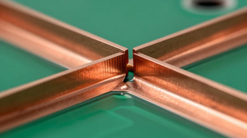
Etching Tolerances and Heavy Copper Geometry
Managing 2oz to 4oz copper requires strict adherence to aspect ratio limitations and advanced etching compensation techniques. As copper weight increases, the side-wall etch rate becomes more pronounced, often leading to trapezoidal trace cross-sections that disrupt impedance matching. Designers must compensate for these lateral etch effects during the artwork generation phase to ensure final trace widths meet functional requirements.
| Copper Weight | Minimum Trace/Space | Etch Factor Allowance |
|---|---|---|
| 2oz (70µm) | 150µm / 150µm | 25-30µm |
| 3oz (105µm) | 200µm / 200µm | 40-50µm |
| 4oz (140µm) | 250µm / 250µm | 60-75µm |
Mitigating Internal Stress and Structural Integrity
High-current pathways in EV BMS systems create localized thermal expansion differentials. When heavy copper is used, the imbalance between the high-mass conductive layers and the low-mass dielectric material often triggers board warping or barrel cracking in vias. To mitigate this, incorporate thermal relief patterns even on high-current planes and utilize symmetrical copper distribution across the Z-axis to maintain stack-up balance.
Key DFM Practices for Heavy Copper
- Is excessive via-stitching required?
Yes, for 3oz+ copper, utilize dense via-stitching arrays with copper-filled or conductive epoxy-filled vias to handle thermal expansion and provide a reliable path for heat dissipation. - How do you prevent delamination?
Ensure that heavy copper layers are buried deep within the stack-up with balanced dielectric thickness to neutralize the mechanical pull of the thick copper foil during reflow. - What is the impact on solder mask?
Heavy copper profiles create high topography; verify solder mask coverage to prevent oxidation of exposed copper edges, which can lead to premature BMS failure.
Strategic Thermal Via Placement and Arrays
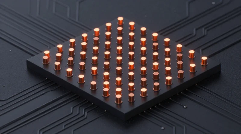
Optimized Thermal Via Array Architectures
In high-density BMS layouts, standard thermal relief patterns are often inadequate for the thermal dissipation requirements of power MOSFETs and shunt resistors. An optimized thermal via array acts as a primary heat-sinking path to the internal copper planes. Designers must move beyond arbitrary placement, adopting a hexagonal close-packed (HCP) arrangement to maximize thermal conductivity while maintaining structural integrity of the PCB substrate.
| Via Feature | Recommended Spec | Performance Impact |
|---|---|---|
| Via Diameter | 0.2mm - 0.3mm | Optimizes plating uniformity. |
| Grid Spacing | 0.5mm - 0.8mm | Balances thermal mass vs. plane integrity. |
| Plating Thickness | 25µm min (1 mil) | Prevents thermal fatigue and micro-cracking. |
Plating Requirements and Reliability
Automotive-grade reliability hinges on the quality of copper deposition within the via barrel. Due to the coefficient of thermal expansion (CTE) mismatch between the FR4 dielectric and copper, inadequate plating can lead to barrel cracking during thermal cycling. For BMS applications, it is standard practice to specify 'capped and plated' (VIPPO) vias or filled vias to prevent solder wicking and ensure a planar surface for component attachment.
- Why is an HCP pattern preferred over a square grid?
Hexagonal close-packing allows for a higher density of vias within the footprint, which reduces thermal resistance by decreasing the distance heat must travel through the dielectric. - How does via filling impact board fabrication?
Using conductive or non-conductive epoxy via filling (followed by copper plating) prevents solder voiding and improves mechanical strength, though it adds cost to the fabrication process. - Is thermal dissipation limited by the via count?
Yes, but there is a point of diminishing returns. Once the thermal resistance of the array matches the internal copper plane impedance, adding more vias offers negligible benefit compared to increasing the copper weight of the connected internal planes.
Mitigating High-Voltage Noise and Signal Integrity

Isolation Strategies for BMS Sensitivity
In EV battery management systems, the challenge lies in protecting sensitive analog front-end (AFE) components from the massive EMI generated by high-voltage contactor switching and PWM-driven motor controllers. The primary mitigation strategy is a strict physical partition of the PCB into 'clean' (low-voltage signal) and 'dirty' (high-voltage power) zones, linked only through optoisolators or digital isolators. Maintaining a minimum creepage and clearance distance, as specified by standards like IEC 60664-1, is not merely a safety requirement but a fundamental DFM rule to prevent parasitic coupling and ensure signal integrity.
Techniques for Signal Path Protection
- Why should differential pairs be prioritized for cell sensing?
Differential signaling provides inherent common-mode noise rejection, which is critical when sensing cell voltages in close proximity to noisy switching MOSFETs. - What role does ground plane splitting play in high-power BMS?
Splitting ground planes prevents return currents from high-power stages from flowing under sensitive analog traces, thereby eliminating ground bounce that could lead to erroneous voltage measurements. - How can vias influence high-frequency EMI?
Via stubs act as antennas for high-frequency noise; minimizing via stub length through back-drilling or blind-via technology is essential for maintaining signal integrity in high-speed communication buses.
Comparison of Noise Mitigation Techniques
| Technique | Primary Benefit | Implementation Complexity |
|---|---|---|
| Galvanic Isolation | Complete EMI/HV barrier | High |
| Differential Routing | Common-mode noise rejection | Medium |
| Keep-out Zones | Physical EMI decoupling | Low |
| Embedded Shielding | Near-field EM suppression | High |
Beyond routing, consider the placement of passive filtering components. Decoupling capacitors must be placed as close as possible to the IC power pins to minimize loop area, which acts as a loop antenna for radiated EMI. By combining these layout constraints with tight impedance control for communication buses, designers ensure the BMS maintains accuracy under extreme operational conditions.
Creepage and Clearance for High-Voltage Safety
Adherence to IPC-2221 and Material Constraints
Designing for high-voltage BMS applications requires strict compliance with IPC-2221 standards, which define the minimum clearance (shortest path through air) and creepage (shortest path along the surface of an insulator) based on voltage potential, pollution degree, and comparative tracking index (CTI) of the substrate material. For automotive environments typically rated for Pollution Degree 2 or 3, engineers must ensure that trace spacing accounts for thermal cycling and vibration, which can degrade air insulation and surface dielectric properties over time.
Design Strategies for Preventing Arcing
| Technique | Primary Function | Implementation Note |
|---|---|---|
| PCB Slotting | Increase Creepage | Milling slots between HV nodes effectively extends the surface path without increasing PCB footprint. |
| Conformal Coating | Environmental Protection | Reduces pollution degree impact; coating must be rated for high dielectric strength. |
| Material Selection | Surface Integrity | Use high-CTI materials (e.g., CTI > 600V) to prevent conductive track formation under high humidity. |
Frequently Asked Questions
- How does pollution degree influence clearance requirements?
Pollution degree defines the amount of conductive contaminants expected in the environment. A higher pollution degree necessitates larger clearance distances to account for potential dust or moisture bridges between conductors. - Why is CTI (Comparative Tracking Index) critical for BMS boards?
CTI measures a material's resistance to surface tracking. In a high-voltage BMS, selecting a high-CTI substrate prevents the creation of permanent carbonized conductive paths if insulation is briefly stressed. - Is slotting effective in high-vibration automotive environments?
Yes, provided the slot geometry is optimized for structural integrity. Using rounded edges in milled slots minimizes mechanical stress concentrations while maximizing effective creepage distance.
Advanced Stack-up Design for BMS Thermal Profiles
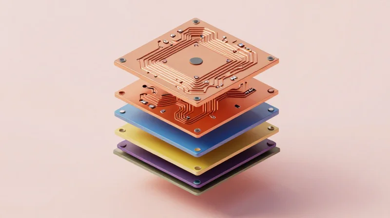
Strategic Stack-up Architecture for Thermal-Signal Balance
In high-voltage Battery Management Systems, the stack-up must simultaneously manage significant thermal flux from MOSFETs and the delicate signal integrity of sensing traces. A balanced symmetrical stack-up is essential to prevent PCB warping during thermal cycling. We recommend placing high-power planes on internal layers adjacent to external copper pours to minimize the thermal impedance path to the heat sink.
| Parameter | Standard FR-4 | High-Tg/Thermal Laminate |
|---|---|---|
| Thermal Conductivity (W/mK) | 0.25 | 0.8 - 2.0 |
| Dielectric Constant (Dk) | 4.5 - 4.8 | 3.5 - 4.2 |
| Glass Transition (Tg) | 130-150°C | 170-200°C |
Dielectric Material Selection
Selecting the correct dielectric is a tradeoff between loss tangent and thermal dissipation. For high-speed BMS communication buses like CAN-FD, low-loss materials are required to maintain signal integrity, while the localized heat zones near current shunts require ceramic-filled laminates. Using a hybrid stack-up—where specific layers utilize high-frequency laminates while internal power layers employ high-thermal-conductivity cores—is an effective DFM strategy for complex designs.
- How do I minimize parasitic capacitance in multi-layer stacks?
Increase the prepreg thickness between high-speed signal layers and ground planes, while keeping the ground planes close to power planes to maintain low-inductance decoupling. - What is the impact of heavy copper on dielectric choice?
Heavy copper (2oz or more) increases the required resin content in the prepreg to ensure proper fill between traces; failure to use high-flow prepreg in these areas leads to structural voids and poor thermal performance. - Is a buried via strategy recommended for BMS?
Yes, using buried vias for signal routing frees up surface real estate for thermal copper pours, allowing for shorter paths to thermal vias and improved heatsinking.
DFM Verification and Simulation Best Practices
Shift-Left Simulation Strategies
The complexity of high-density BMS layouts necessitates moving verification from post-layout validation to pre-layout planning. By performing thermal modeling and SI/PI simulation at the component placement stage, designers can identify potential hotspots and signal crosstalk before routing begins, significantly reducing iterations and costly re-spins.
Verification Workflow Comparison
| Analysis Type | Primary Goal | Verification Stage | Key Metric |
|---|---|---|---|
| Thermal Modeling | Component Junction Temp | Placement & Routing | Degrees Celsius |
| Signal Integrity (SI) | Data Line Fidelity | Pre-Layout & Post-Layout | Eye Diagram Aperture |
| Power Integrity (PI) | Voltage Ripple/Droop | Stack-up Design | Impedance Profile (Ohms) |
Best Practices for Simulation Accuracy
- How do I ensure simulation accuracy for high-density BMS boards?
Always use real-world environmental boundary conditions, including actual airflow rates and enclosure thermal resistances, rather than defaulting to generic convection coefficients. - Why should I simulate PI before routing?
Simulating PDN (Power Distribution Network) impedance early ensures the board stack-up and plane capacitance are sufficient to handle high-frequency switching transients from BMS controllers, preventing unexpected voltage ripples. - What is the critical step in validating high-speed sensing lines?
Perform differential pair skew analysis post-layout to ensure trace length matching is preserved, as even sub-millimeter mismatches can degrade signal integrity in dense EV sensing interfaces.
Automation Integration
Automate verification checks by embedding Design Rule Checks (DRC) directly into the CAD environment. Utilize scripted batch processes to monitor thermal clearance violations during every save operation, ensuring that design guidelines are enforced automatically as the PCB complexity increases.
Collaborating with Fabrication Partners
Bridging Design Intent and Manufacturing Reality
Achieving first-pass success for high-density BMS layouts relies on proactive communication. Rather than providing only Gerber files, design engineers must provide comprehensive fabrication notes that detail thermal relief strategies, impedance control requirements, and specific material tolerances. Open dialogue with your manufacturer's DFM team during the preliminary design stage prevents costly last-minute adjustments to copper weights or stack-up architectures that could otherwise compromise your thermal dissipation goals.
Key Data Package Requirements
- Impedance Control
Explicitly define target impedance profiles for high-speed communication traces (e.g., CAN bus, Daisy Chain), including required stack-up layer sequences and reference plane conditions. - Thermal Management Features
Clearly annotate locations for thermal vias and specify plating thickness requirements to ensure efficient heat transfer from MOSFETs and shunt resistors to internal ground planes. - Material Specification
Provide specific Tg (Glass Transition Temperature) and CTI (Comparative Tracking Index) values to match the rigorous reliability demands of automotive-grade BMS hardware.
Communication Matrix: Fabrication vs. Design
| Design Constraint | Fabrication Impact | Communication Priority |
|---|---|---|
| Copper Weight | Trace etch factor and thermal mass | High: Define for power paths |
| Via-in-pad | Plating voids and solder wicking | Critical: Specify fill/cap methods |
| Conformal Coating | Surface contamination risks | Medium: Define mask keep-out areas |
Managing DFM Sign-off Processes
Always request a formal DFM report before production begins. Focus these reviews on your most critical areas: high-voltage creepage distances, thermal via distribution, and impedance matching on differential pairs. When the manufacturer flags a potential violation, assess the impact on your SI/PI simulation model before approving any deviation; a seemingly minor change to trace width or clearance can inadvertently create significant EMI signatures or thermal bottlenecks in high-density EV battery monitoring systems.
Optimizing a BMS PCB requires an uncompromising balance between thermal efficiency, signal purity, and strict safety standards. By implementing these advanced DFM strategies, engineering teams can significantly reduce failure rates and ensure long-term stability in demanding EV environments. Ready to take your BMS design to the next level? Contact our engineering team today to review your current layout or schedule a design-for-manufacturing audit.
