
In the fast-evolving landscape of Vehicle-to-Everything (V2X) communication, the margin for error is non-existent. As these modules demand increasing data throughput and robust connectivity, engineers face the dual challenge of maintaining signal integrity while managing extreme thermal loads. This guide provides an authoritative breakdown of the design-for-manufacturing (DFM) processes essential for high-reliability automotive PCBs.
The Anatomy of V2X Reliability

Engineering for Mission-Critical V2X Connectivity
Vehicle-to-Everything (V2X) communication demands ultra-low latency and absolute signal reliability. Because these systems operate in safety-critical roles, the PCB architecture must account for high-frequency attenuation, impedance discontinuities, and extreme thermal cycling that can lead to intermetallic compound fatigue and material delamination.
Comparison of Standard vs. High-Reliability V2X PCB Requirements
| Requirement Category | Standard Automotive PCB | High-Reliability V2X PCB |
|---|---|---|
| Dielectric Loss | Standard FR-4 / Mid-loss | Ultra-low loss / PTFE-based |
| Operating Temperature | -40°C to +105°C | -40°C to +150°C (AEC-Q100 Grade 0) |
| Via Integrity | Standard Through-hole | Back-drilled / Micro-vias with filled epoxy |
| Copper Weight | 1 oz | 2 oz+ for improved thermal dissipation |
Frequently Asked Questions on V2X Design
- Why is impedance control more critical in V2X than in standard infotainment systems?
V2X modules utilize high-frequency signals (5.9 GHz DSRC or C-V2X bands) where signal reflections caused by impedance mismatches can cause packet loss and link-margin reduction, potentially compromising safety-critical data exchange. - How does thermal management impact signal integrity in V2X boards?
Increased heat alters the dielectric constant of PCB laminates over time. This shift changes the signal propagation speed, which can cause phase mismatches and signal degradation in high-speed digital interfaces.
Optimizing Multi-Layer Stack-ups for High-Speed Data
Core Principles of V2X Stack-up Architecture
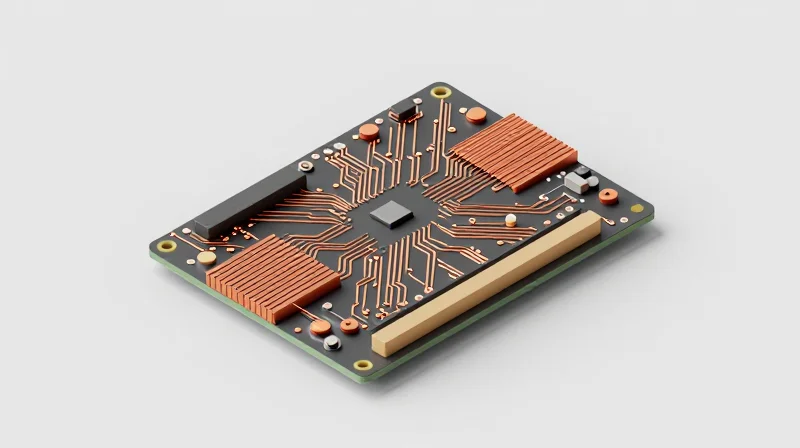
For V2X modules operating at 5.9 GHz and beyond, the stack-up must prioritize controlled impedance stability and minimal return loss. A symmetric stack-up is mandatory to prevent board warping during extreme automotive thermal cycling. Engineers should implement at least a 6-to-10 layer structure, where high-speed differential pairs are sandwiched between solid reference planes to provide a continuous return path and minimize EMI radiation.
Comparative Analysis: Dielectric Selection for High-Speed Reliability
| Material Type | Dielectric Constant (Dk) | Dissipation Factor (Df) | Automotive Suitability |
|---|---|---|---|
| Standard FR-4 | 4.4 - 4.8 | 0.020 | Low (High signal loss) |
| High-Tg FR-4 | 4.1 - 4.4 | 0.015 | Moderate (Better thermal stability) |
| PTFE-filled Ceramic | 3.0 - 3.6 | 0.002 | High (Superior for mmWave V2X) |
Mitigating Crosstalk and Signal Degradation
To maintain signal integrity in dense V2X layouts, designers must strictly adhere to the '3W rule' for trace spacing to reduce coupled noise. Furthermore, stitching vias should be strategically placed near signal via transitions between reference planes to minimize discontinuous return current paths. Using a 'ground-signal-signal-ground' (GSSG) configuration in critical high-frequency zones provides optimal shielding against substrate-coupled noise.
Design FAQ: Stack-up Best Practices
- Why is board symmetry critical for V2X reliability?
Asymmetric stack-ups lead to uneven copper distribution, causing mechanical stress and board bowing during automotive thermal shock testing, which can crack vias. - How does reference plane discontinuity impact performance?
Splits in reference planes force return currents to take long, inductive paths, significantly increasing electromagnetic emissions and causing signal reflections. - What is the recommended approach for thermal management in the stack-up?
Utilize dedicated internal copper planes as heat spreaders and incorporate thermal via arrays directly under high-power RF ICs to conduct heat to the bottom mounting surface.
Mastering Controlled Impedance in Manufacturing
Mastering Controlled Impedance in Manufacturing
Controlled impedance is the cornerstone of signal integrity in V2X applications, where millimeter-wave frequencies demand absolute consistency in transmission line geometry. To achieve the required tolerances (typically ±5% to ±10%), manufacturers must move beyond standard fabrication methods toward a design-for-manufacturing (DFM) workflow that accounts for the dynamic relationship between trace width, dielectric height, and copper thickness under harsh automotive thermal profiles.
Critical DFM Strategies for Impedance Stability
- Accounting for Copper Etch Factor
Standard etching creates trapezoidal cross-sections rather than perfect rectangles. DFM rules must compensate by adjusting the artwork width to ensure the final trace impedance matches the design intent after chemical depletion. - Dielectric Constant (Dk) Stability
V2X modules experience temperatures from -40°C to +125°C. Select PCB core materials with a stable Dk over this range to prevent frequency shifts in antenna arrays and high-speed data buses. - Reference Plane Continuity
Ensure zero discontinuities in the ground planes beneath signal lines. Even small voids or via-stitching gaps can cause localized impedance spikes, leading to unacceptable signal reflections.
| Parameter | Control Requirement | Impact on V2X Performance |
|---|---|---|
| Trace Width | ±0.5 mil | Prevents impedance mismatch at Gbit rates |
| Dielectric Height | ±3% tolerance | Stabilizes characteristic impedance across boards |
| Surface Finish | ENEPIG/Immersion Silver | Minimizes skin-effect losses at 5.9GHz |
Manufacturing Feedback Loop
For high-reliability V2X, relying solely on theoretical simulations is insufficient. Engineers must mandate the inclusion of TDR (Time-Domain Reflectometry) coupons on the board panel to provide empirical verification of impedance profiles before final assembly. This data should feed back into the stack-up design to calibrate future fabrication iterations, ensuring the PCB consistently meets the strict link-budget requirements mandated by automotive standards like IEEE 802.11p or C-V2X.
Advanced Thermal Dissipation Strategies
Advanced Thermal Dissipation Strategies
V2X modules often face high power density within thermally constrained, compact automotive enclosures. To mitigate heat buildup, engineers must move beyond passive cooling by integrating high-conductivity substrate materials with strategic thermal via arrays that act as vertical heat pipes. This design methodology ensures that the junction temperature of RF and processing components remains well within the safety margins defined by automotive qualification standards like AEC-Q100.
Comparative Thermal Management Materials
| Material Type | Thermal Conductivity (W/mK) | Primary Application |
|---|---|---|
| Standard FR-4 | 0.25 | General logic circuits |
| High-Tg Polyimide | 0.4 - 0.6 | High-temp engine environments |
| Metal-Core PCB (IMS) | 1.0 - 3.0 | Power conversion modules |
| Ceramic Substrates | 20 - 200 | Critical RF/Power amplifiers |
Via Array Optimization and Heat Spreading
Thermal via arrays must be meticulously placed beneath the thermal pads of surface-mount components. For optimal performance, these vias should be copper-filled and capped to allow for direct solder mounting, effectively creating a low-thermal-resistance path to the internal ground planes or external heat sinks. Using a staggered array pattern instead of a grid further minimizes the impact on board structural integrity while maximizing heat distribution.
Frequently Asked Questions
- Why is copper-filling preferred over standard plating for thermal vias?
Copper-filling provides a solid thermal path that prevents the entrapment of outgassing flux and significantly lowers the thermal resistance compared to hollow, plated-through holes. - How do heat spreaders impact impedance control?
While heat spreaders improve thermal dissipation, they can act as unwanted reference planes, altering trace capacitance. DFM rules must account for these proximity effects to maintain signal integrity. - What is the recommended density for thermal via arrays?
A density of 20-30% copper coverage in the thermal pad area is generally optimal, balancing heat transfer efficiency against the risks of delamination during reflow soldering.
Ensuring Solder Joint Integrity under Mechanical Stress
Mitigating CTE Mismatch in High-Reliability V2X Environments
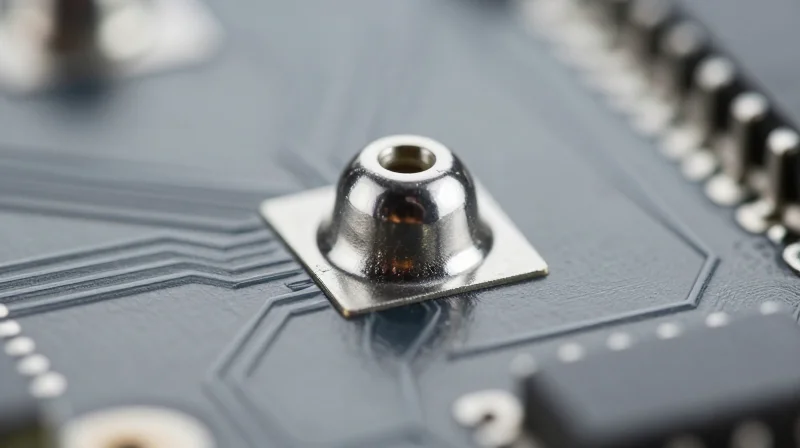
The operational lifespan of V2X modules is frequently limited by solder joint fatigue caused by the coefficient of thermal expansion (CTE) mismatch between ceramic/silicon components and FR-4 or hybrid laminate substrates. To ensure long-term interconnect integrity under extreme automotive temperature cycling (-40°C to +125°C), DFM strategies must prioritize substrate materials with lower CTE values or utilize constrained-core technology to neutralize board-level strain.
| Material Type | CTE (ppm/°C) | Suitability for V2X |
|---|---|---|
| Standard FR-4 | 14-17 | Low (High risk of delamination) |
| High-Tg Polyimide | 12-14 | Medium (Better thermal stability) |
| Ceramic-Filled PTFE | 8-10 | High (Excellent match to chip scale) |
Vibration Resistance and Mechanical Reinforcement
V2X PCBs mounted in chassis-integrated locations are subject to severe harmonic vibration profiles. Solder joints for large BGA (Ball Grid Array) packages are particularly susceptible to crack propagation under stress. Implementing mechanical reinforcement, such as corner staking or full underfill, is critical for high-mass components. Furthermore, symmetrical component placement across the PCB neutralizes localized board warping during thermal expansion cycles.
Best Practices for Joint Reliability
- How does PCB thickness influence solder fatigue?
Thicker boards exhibit higher stiffness, increasing the bending moment on solder joints. Limit aspect ratios and keep boards thin where possible. - Should non-solder mask defined (NSMD) pads be used?
Yes, NSMD pads generally provide better solder anchoring and flexibility, which is preferred for high-stress automotive environments compared to SMD pads. - Is lead-free (SAC305) adequate for V2X?
While standard, SAC305 can be brittle. Consider adding dopants like bismuth or nickel to the solder alloy to improve drop-shock and vibration toughness.
DFM Rules for PCB Fabrication and Assembly
Critical DFM Rules for High-Reliability V2X Assemblies
Designing for high-reliability V2X systems requires a departure from standard consumer electronics specifications. By enforcing strict DFM rules at the layout stage, engineers can minimize manufacturing-induced defects such as copper delamination, solder bridging, and signal degradation caused by improper via structures.
Advanced Manufacturing Guidelines
| Feature | Recommended DFM Practice | Reliability Benefit |
|---|---|---|
| Edge Plating | Extend copper 0.2mm from edge, use non-conductive fill | Prevents shorting and enhances structural integrity |
| Via-in-Pad | IPC-4761 Type VII (capped and plated) | Prevents solder wicking and ensures flat surface |
| Panelization | Tab-routing with breakaway perforated edges | Minimizes mechanical stress during depanelization |
Technical Best Practices for Via-in-Pad and Plating
The use of via-in-pad is essential for high-density V2X modules to minimize parasitic inductance. However, improper application leads to solder starvation. Always specify conductive or non-conductive epoxy filling followed by copper plating (capped vias) to provide a planar mounting surface for BGA components.
- How does edge plating improve reliability?
Edge plating provides a continuous electrical path along the board perimeter, which is critical for shielding against EMI in V2X environments and improving PCB stiffness against mechanical vibration. - What is the optimal approach for panelization?
Avoid V-score cutting for boards carrying sensitive RF components; use laser-cut or router-tab methods to reduce mechanical shock transfer that could fracture fragile ceramic capacitors or solder joints. - How to avoid solder wicking in via-in-pad?
Strict adherence to IPC-4761 Type VII via protection is mandatory. This process creates a flat, fully capped via that prevents solder from flowing into the barrel during reflow.
Testing and Validation for Automotive Standards
Validating Against AEC-Q and ISO Standards
Verification of V2X PCBs requires a multi-stage approach that validates DFM assumptions against the rigorous AEC-Q100/200 and ISO 26262 functional safety requirements. While simulation tools predict behavior under ideal conditions, physical validation must confirm signal integrity (SI) and thermal stability across the full automotive operating temperature range, typically -40°C to +125°C.
| Test Category | Standard | Primary Metric |
|---|---|---|
| Thermal Cycling | AEC-Q200 | Solder Joint Fatigue / CTE Match |
| Signal Integrity | ISO 16750-2 | Eye Diagram Mask / Bit Error Rate |
| Vibration/Shock | AEC-Q100 | Interconnect Resistance Shifts |
| Functional Safety | ISO 26262 | Failure Mode Diagnostic Coverage |
Bridging Simulation and Physical Testing
A common failure in V2X design is the disconnect between finite element analysis (FEA) predictions and board-level hardware testing. To mitigate this, engineers must employ correlation testing, where real-world thermal camera data and high-speed oscilloscope measurements are fed back into simulation models to refine future DFM rules.
- How do we validate thermal dissipation models?
Use infrared thermography during high-load V2X radio transmission to verify that hot spots match FEA heat-map predictions within a 5% margin. - What is the role of TDR in high-speed validation?
Time Domain Reflectometry (TDR) is critical to verify impedance control on high-frequency V2X traces, ensuring that PCB manufacturing variations do not degrade signal quality. - Does simulation replace physical reliability testing?
No; simulations identify design risks, but environmental stress screening (ESS) is essential to detect latent manufacturing defects such as delamination or via wall cracking.
Data-Driven Compliance Workflow
1. Baseline Simulation (Pre-Layout) -> 2. Design Review (DFM/SI Rules) -> 3. Prototype Fabrication -> 4. Correlation Testing (Thermal/Signal) -> 5. Final Compliance Stress ScreeningSuccessfully designing for V2X requires a holistic approach that fuses high-speed signal integrity with rugged mechanical reliability. By adhering to these advanced DFM principles, your team can accelerate time-to-market while ensuring long-term performance in the field. Ready to optimize your next automotive project? Contact our engineering team today for a comprehensive design review.
