
As the automotive industry shifts toward autonomous and hyper-connected ecosystems, the communication protocols powering these vehicles are undergoing a seismic transformation. For hardware engineers, this transition from legacy DSRC to high-performance C-V2X represents a fundamental change in PCB architecture requirements. In this deep dive, we examine the technical hurdles and design strategies necessary to build the next generation of reliable, high-speed automotive connectivity.
Understanding the Shift: From DSRC to C-V2X
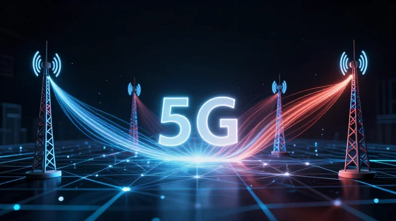
The Legacy of DSRC: Foundations of Vehicle Connectivity
Dedicated Short-Range Communications (DSRC) served as the initial bedrock for vehicular connectivity, relying on the IEEE 802.11p standard. Designed as an evolution of Wi-Fi for mobile environments, DSRC focused on low-latency safety-critical messages. However, its reliance on localized, ad-hoc networking limited its scalability and integration capabilities in the burgeoning era of smart cities and high-bandwidth autonomous vehicle data demands.
The C-V2X Advantage: Scalability and Future-Proofing
Cellular Vehicle-to-Everything (C-V2X) introduces a paradigm shift by leveraging established cellular infrastructures (LTE-V2X and 5G-NR V2X). Unlike DSRC, C-V2X offers a robust evolutionary path that benefits from the massive global investment in cellular technology, providing superior range, reliability, and the non-line-of-sight performance necessary for advanced ADAS features.
| Feature | DSRC (802.11p) | C-V2X (3GPP) |
|---|---|---|
| Standards Base | IEEE 802.11 | 3GPP (Rel 14/15/16) |
| Infrastructure | Standalone/Roadside Units | Cellular Network/Direct |
| Performance | Short-Range/Ad-hoc | Long-Range/Reliable |
| Future-Proofing | Static | 5G/Beyond Evolution |
Critical Comparison FAQ
- Why is the industry moving away from DSRC?
The transition is driven by the superior technical performance of 5G-NR V2X, the commercial viability of leveraging cellular ecosystems, and the need for higher data throughput that DSRC cannot support. - How does C-V2X impact PCB design?
C-V2X necessitates more complex RF front-end modules, enhanced thermal management for 5G processing chips, and tighter integration of multi-antenna arrays compared to the relatively simpler DSRC radio hardware.
Core Architectural Challenges in Modern V2X PCBs
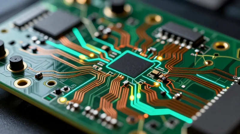
Signal Integrity in the 5G Era
The shift toward 5G-NR frequency bands for C-V2X operations creates significant challenges for PCB layout design. As frequencies rise, trace losses become exponentially more difficult to manage due to the skin effect and dielectric absorption. Designers must move away from standard FR-4 laminates in favor of low-loss, high-frequency materials such as PTFE or hydrocarbon-ceramic laminates. Furthermore, ensuring impedance matching across high-speed digital interfaces and RF front-ends is critical, as even minor impedance discontinuities can lead to excessive signal reflection and packet loss in safety-critical vehicle-to-infrastructure communication.
Thermal Management and Electromagnetic Interference (EMI)
Modern V2X modules pack significant processing power and RF amplification into compact form factors, leading to intense localized heat dissipation. Thermal management is no longer an afterthought; it is a primary architectural constraint. High-density interconnect (HDI) designs must prioritize thermal vias and integrated heat spreaders to prevent board delamination or component throttling. Concurrently, the proximity of sensitive GPS/GNSS receivers to high-power 5G transmitters demands rigorous EMI shielding. Implementing multi-layer isolation, substrate-integrated waveguides (SIW), and strategic ground plane stitching is essential to maintain signal purity in the congested electromagnetic environment of a modern vehicle.
Comparative PCB Design Metrics: DSRC vs. C-V2X
| Feature | DSRC (5.9 GHz) | C-V2X (5G NR / PC5) |
|---|---|---|
| Frequency Range | Narrow (5.85-5.925 GHz) | Broad (5.9 GHz up to mmWave) |
| Dielectric Requirement | Standard FR-4 / Low Cost | Advanced Low-Loss Laminates |
| EMI Sensitivity | Moderate | High (Multi-band interference) |
| Thermal Density | Low to Moderate | High (5G Baseband processing) |
Frequently Asked Questions
- Why is FR-4 insufficient for C-V2X designs?
FR-4 exhibits high dielectric loss at the higher frequencies mandated by 5G NR, causing signal attenuation that degrades the reliable communication range necessary for autonomous vehicle safety. - How does C-V2X affect PCB stack-up density?
C-V2X requires complex multi-layer stack-ups to allow for isolated RF paths and high-speed digital routing, necessitating HDI (High-Density Interconnect) technology to maintain the required board miniaturization.
The Impact of 5G Integration on Board Layout
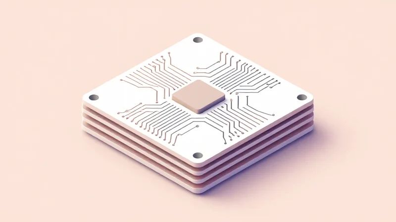
Optimizing Trace Routing and Stack-up for 5G Frequencies
Transitioning to 5G New Radio (NR) requires addressing the extreme sensitivity of high-frequency signals to board geometry. Designers must move beyond standard FR-4 materials toward low-loss substrates, such as PTFE or hydrocarbon-ceramic laminates, to minimize dielectric loss at sub-6GHz and mmWave frequencies. Controlled impedance routing has become significantly more stringent; trace widths and spacing must be maintained with sub-micron precision, and via stubs must be back-drilled to prevent resonant reflections that degrade signal integrity.
Comparative Design Constraints: DSRC vs. 5G V2X
| Parameter | DSRC (5.9 GHz) | 5G NR V2X (Sub-6/mmWave) |
|---|---|---|
| Substrate Material | Standard FR-4 / Mid-loss | Ultra-low loss (PTFE/Ceramic) |
| Via Design | Standard thru-hole | Back-drilled / Micro-vias |
| Thermal Management | Passive cooling | Advanced heat-spreading thermal vias |
| Trace Routing | Flexible constraints | Strict impedance-controlled stripline |
Antenna Placement and EMI Mitigation
In a 5G-enabled V2X architecture, the antenna-to-transceiver path length must be minimized to combat path loss. This often dictates a 'distributed architecture' where front-end modules are placed in immediate proximity to the antenna arrays. Furthermore, isolation between multiple antennas—required for MIMO (Multiple Input, Multiple Output) performance—demands sophisticated electromagnetic shielding and carefully calculated physical separation to mitigate cross-talk and preserve SNR.
FAQs on 5G V2X Integration
- Why is standard FR-4 insufficient for 5G V2X?
FR-4 possesses a high dissipation factor (Df) that leads to excessive signal attenuation at frequencies above 6GHz, rendering it ineffective for high-bandwidth 5G V2X applications. - How does back-drilling improve signal integrity?
Back-drilling removes the unused portion of a plated through-hole via, eliminating the 'stub' that can act as an antenna and cause unwanted signal resonance at high frequencies. - What role does thermal management play in 5G board layout?
5G power amplifiers generate high localized heat density; efficient board layout requires integrated thermal vias and copper planes to dissipate heat, preventing frequency drift and degradation of active components.
Material Selection: Balancing RF Performance and Cost
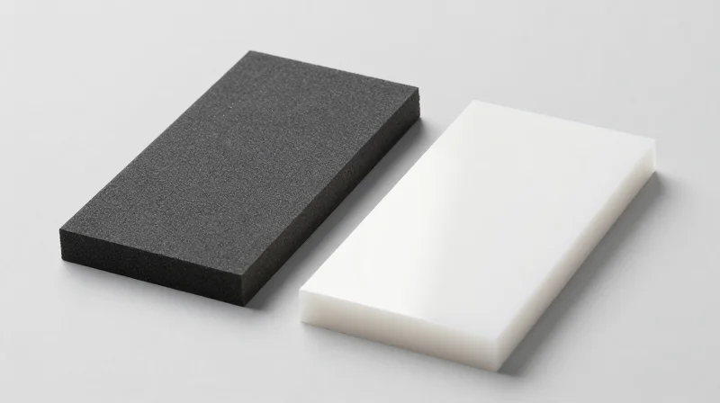
Navigating High-Frequency Material Requirements
As V2X connectivity transitions toward 5G-enabled C-V2X, signal integrity at high frequencies (5.9GHz and beyond) has become the primary constraint. Engineers must prioritize materials with low Dielectric Constant (Dk) and ultra-low Dissipation Factor (Df) to minimize insertion loss. While PTFE-based laminates offer superior electrical performance, they are often cost-prohibitive for high-volume automotive production, leading designers to favor hybrid stack-up approaches.
Material Comparison Matrix
| Material Class | Dielectric Loss (Df) | Cost Profile | V2X Application |
|---|---|---|---|
| Standard FR-4 | High (>0.015) | Low | Not suitable for RF |
| High-Tg/Low-Loss FR-4 | Medium (0.005-0.010) | Moderate | Low-frequency control |
| PTFE/Ceramic Filled | Ultra-Low (<0.002) | Very High | Antenna & RF Front-End |
| Hybrid Laminates | Low (Variable) | Balanced | Main V2X Processing |
Strategic Cost-Performance Trade-offs
- Why is a hybrid stack-up preferred for V2X?
Hybrid stack-ups utilize high-performance, low-loss materials only in the critical high-frequency signal layers, while using cost-effective materials for inner power and ground planes, significantly reducing total BOM cost. - How does surface roughness impact C-V2X designs?
At higher frequencies, the 'skin effect' causes current to flow along the surface of traces. Using low-profile or rolled-annealed copper foil reduces insertion loss, even if the base substrate is moderately priced. - Does thermal stability affect material selection?
Yes, V2X modules often reside in high-temperature engine compartments. Materials must exhibit a low Coefficient of Thermal Expansion (CTE) to prevent mechanical stress on high-density interconnects (HDI) during thermal cycling.
Ultimately, the evolution of V2X requires moving away from one-size-fits-all board materials. By adopting a tiered material strategy, manufacturers can ensure the reliability of C-V2X communications while maintaining a viable path for the mass-market automotive industry.
Power Distribution Networks in High-Density Systems
Managing Transient Response and Low Impedance
In C-V2X architectures, processors frequently transition between sleep and burst processing modes, creating rapid di/dt events. A robust PDN must maintain ultra-low impedance across a broad frequency range to prevent voltage droop, which can lead to intermittent system crashes or bit errors in time-sensitive V2X communication links.
Strategies for High-Density Power Integrity
| Design Strategy | Impact on V2X Performance | Implementation Tip |
|---|---|---|
| Embedded Capacitance | Reduces high-frequency impedance | Use thin dielectric core layers |
| Decoupling Placement | Mitigates switching noise | Mount caps on bottom side under SoC |
| Plane Optimization | Minimizes loop inductance | Adopt narrow vertical stackup geometry |
Frequently Asked Questions
- How does C-V2X change PDN requirements compared to DSRC?
C-V2X utilizes more complex 5G baseband processors requiring higher current densities and stricter voltage tolerance, whereas DSRC systems generally operated with lower power throughput. - What is the primary risk of a poorly designed PDN?
The primary risk is transient voltage noise that compromises the Signal-to-Noise Ratio (SNR) of RF front-ends, leading to packet loss in critical vehicle safety communications. - Why is vertical plane spacing crucial?
Reducing the distance between power and ground planes increases inter-plane capacitance, which is vital for filtering high-frequency noise that decoupling capacitors cannot suppress effectively.
Addressing Thermal Constraints in Enclosed Automotive Environments
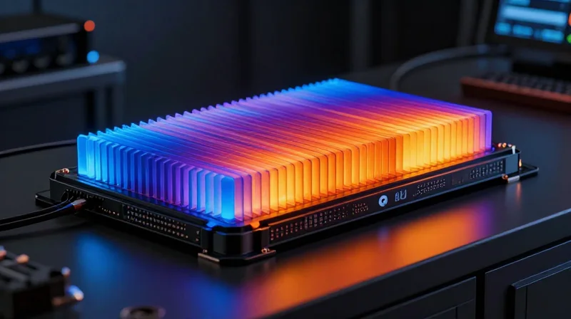
Mitigating Thermal Throttling in High-Density TCUs
Automotive V2X telematics control units (TCUs) face extreme thermal challenges due to the convergence of high-performance C-V2X baseband processors and the confined, fanless environments of vehicle chassis. When localized temperatures exceed set thresholds, the processor initiates frequency scaling, known as thermal throttling, which significantly degrades latency and throughput. Designing for effective heat dissipation requires a multi-layered approach that integrates advanced thermal interface materials (TIM), strategic component placement, and PCB-level heat-spreading technologies.
Advanced Thermal Dissipation Strategies
- Thermal Vias and Copper Pours
Utilizing high-density thermal via arrays beneath the processor package acts as a conduit to move heat to the bottom ground plane, which serves as a secondary radiator for the PCB. - Phase-Change TIMs
Implementing phase-change material as a thermal interface between the SoC and the chassis heat sink provides superior longevity and performance stability compared to standard silicone-based greases in automotive cycles. - Staggered Component Placement
Distributing high-heat sources like power management ICs (PMICs) and RF front-end modules away from the baseband processor prevents localized thermal 'hot spots' that compound cooling complexity.
| Strategy | Performance Impact | Complexity |
|---|---|---|
| Active Thermal Vias | High Efficiency | Low |
| Copper Heat Sinks | Moderate Efficiency | Medium |
| Chassis Integration | Very High Efficiency | High |
Ensuring Long-term Reliability
To ensure reliable V2X communication in extreme environments, designers must treat the entire chassis as a heat exchanger. The mechanical housing should feature an integrated heat-pipe structure or machined aluminum fins that physically bridge to the PCB heat-spreader. Validation must involve IR thermal imaging under peak-load scenarios to ensure the device remains below critical junction temperature (Tj) limits, avoiding not only performance throttling but also permanent degradation of solder joints and dielectric layers caused by continuous thermal cycling.
Security and Reliability: Designing for Automotive Grade Standards
Implementing ISO 26262 Functional Safety
To meet Automotive Safety Integrity Level (ASIL) requirements, V2X PCB design must move beyond standard industrial practices. Developers must implement hardware redundancy and sophisticated diagnostic coverage to ensure the system remains in a safe state during failure modes. This includes the integration of external watchdog timers, independent power monitoring, and ECC (Error Correction Code) memory to protect data integrity against transient faults.
Hardware-Anchored Security Architectures
As V2X connectivity expands, protecting vehicle-to-everything communication from malicious interference is critical. Modern V2X designs incorporate Hardware Security Modules (HSMs) directly on the PCB. These silicon-based roots of trust handle cryptographic key management, secure boot processes, and message signing without exposing sensitive keys to the main application processor. Shielding these components within multi-layer PCB stacks is essential to prevent side-channel attacks.
| Safety/Security Feature | PCB Implementation Strategy | Target Goal |
|---|---|---|
| HSM Integration | Dedicated isolated silicon area | Cryptographic security |
| Redundancy | Dual-path signal routing/Power domains | ISO 26262 ASIL Compliance |
| EMI/EMC Hardening | Ground plane stitching/shielding cages | Signal integrity reliability |
Key Considerations for Automotive Reliability
- How does PCB layout impact functional safety?
Layout design dictates failure propagation; physical separation between safety-critical circuits and high-speed communication interfaces is mandatory to avoid common-cause failures. - What is the role of the Hardware Security Module (HSM)?
The HSM acts as a secure cryptographic vault, ensuring that V2X messages (like BSMs) are authenticated, preventing spoofing and unauthorized vehicle control. - How is environmental reliability verified?
Boards must undergo accelerated life testing (ALT) and vibration profile analysis to ensure that solder joints and component mounts survive the harsh thermal cycling inherent in automotive environments.
Future-Proofing Your V2X Hardware Roadmap
Architectural Agility Through Modular Design
To mitigate the risk of premature obsolescence, engineers must prioritize modular PCB designs. Decoupling the baseband processing unit from the RF front-end allows manufacturers to swap connectivity modules as standards evolve from legacy DSRC to advanced 5G-NR V2X without requiring a complete redesign of the host PCB. Utilizing standardized high-speed mezzanine connectors ensures that communication interfaces remain future-proof while simplifying supply chain management.
Strategies for Hardware Scalability
| Strategy | Design Benefit | Future-Proofing Impact |
|---|---|---|
| Software-Defined Radio | Programmable signal processing | Adapts to evolving protocol standards |
| Mezzanine Connectivity | Modular hardware interfaces | Facilitates hardware upgrades without PCB overhaul |
| High-Frequency PCB Materials | Low-loss dielectric substrates | Supports higher carrier frequencies (mmWave) |
Key Considerations for Long-Term V2X Deployment
- How can designers handle frequency migration?
Utilize wideband antenna designs and programmable RF front-ends that can span the 5.9GHz spectrum and beyond to accommodate regional regulatory changes. - Why is board space allocation critical?
Allocating extra surface area for future co-processors or hardware security modules (HSMs) ensures that security updates or increased computational loads do not necessitate a total layout re-spin. - What role does signal integrity play?
Implementing advanced routing techniques and low-loss substrates now prevents performance bottlenecks when transitioning to the higher data rates required by Cooperative Perception and autonomous driving applications.
Ultimately, the longevity of V2X hardware rests on the ability to isolate critical communication paths from the rapidly changing radio-frequency environment. By adopting a 'compute-first' design philosophy, where the primary telematics processor remains consistent while the connectivity engine remains modular, OEMs can maintain compliance with evolving automotive safety standards while minimizing long-term integration costs.
The transition to C-V2X is more than a protocol change; it is a mandate for more sophisticated, resilient, and performant PCB design. By prioritizing signal integrity, thermal management, and material science today, engineers can lead the charge in the connected vehicle revolution. Are you ready to optimize your next-gen automotive hardware? Contact our engineering team today to discuss your connectivity design challenges.
