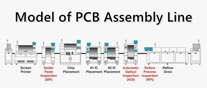
Automatic Inspection Assembly Line Control PCB Solution
2025.08.01
In today's fast-paced manufacturing landscape, precision, efficiency, and reliability are paramount. The backbone of any advanced automated assembly line lies in its control systems, and at the heart of these systems are sophisticated Printed Circuit Boards (PCBs). Zero One Solution Limited, a leader in rapid prototyping and one-stop PCB services since 2011, understands this critical need. We are strategically positioned to empower industries to achieve unprecedented levels of automation through our specialized Automatic Inspection Assembly Line Control PCB Solutions. How can your production line benefit from cutting-edge PCB technology designed for seamless integration and robust performance?
The Evolution of Automated Assembly Lines
The relentless pursuit of efficiency and precision has fundamentally reshaped manufacturing, propelling the evolution of assembly lines from manual labor to sophisticated automated systems. This transformation, deeply rooted in the industrial revolutions, now hinges on advanced control mechanisms, with Printed Circuit Boards (PCBs) serving as the indispensable neural network enabling the intricate dance of modern automatic inspection and assembly. The journey from human-centric production to fully automated lines underscores a critical demand for robust, high-performance PCB solutions capable of managing complex data flows, executing precise commands, and facilitating real-time quality control.
From Manual to Mechanized: The Dawn of Automation Early assembly lines, pioneered by Henry Ford, revolutionized production by segmenting tasks and minimizing movement. While revolutionary for their time, these lines were inherently labor-intensive and susceptible to human error and fatigue. The mid-20th century introduced rudimentary automation with pneumatic and hydraulic systems, offering improved speed but lacking the flexibility and precision required for complex modern manufacturing.
The Rise of Semi-Automated Systems: Bridging the Gap The advent of electronics and early computing marked a pivotal shift towards semi-automated assembly. Programmable Logic Controllers (PLCs) and basic robotic arms began to integrate into production, handling repetitive and dangerous tasks. This phase significantly boosted throughput and consistency, yet human intervention remained crucial for setup, quality inspection, and troubleshooting, highlighting a need for more autonomous control.
Fully Automated Lines: The Digital Transformation Today's fully automated assembly lines are a testament to the digital age, characterized by seamless integration of robotics, advanced sensors, machine vision, and AI-driven inspection systems. These lines operate with minimal human oversight, capable of self-optimization, rapid reconfiguration, and performing intricate tasks with sub-millimeter precision. The core enabler of this sophistication is the underlying PCB infrastructure, which processes vast amounts of data, orchestrates complex robotic movements, and ensures real-time quality assurance at every stage.
The Imperative for Advanced PCB Solutions The increasing complexity and speed of modern automated assembly lines necessitate PCBs that go beyond basic connectivity. They demand high-density interconnect (HDI) designs, multi-layer architectures for signal integrity, robust power delivery, and advanced thermal management. Furthermore, the integration of high-speed communication interfaces (e.g., Industrial Ethernet, EtherCAT), powerful microcontrollers, and dedicated signal processing units on these PCBs is crucial for handling the massive data streams generated by inline inspection systems and executing precise control commands for robotic manipulators. Without these sophisticated PCB solutions, the promise of Industry 4.0 – characterized by smart factories and autonomous production – would remain unfulfilled.
Automation Phase
Key Characteristics
Impact on Production
PCB Role (Evolutionary)
Manual
Human-centric, labor-intensive, simple tools
Low consistency, high error rate, slow
None (or rudimentary wiring)
Semi-Automated
PLCs, basic robotics, human oversight
Improved speed & consistency, still human-dependent
Basic control boards, relay logic PCBs
Fully Automated
Advanced robotics, AI/ML, sensor networks, minimal human intervention
High speed, high precision, low error rate, flexible
Core Components of Automatic Inspection Assembly Line Control PCBs
Automatic Inspection Assembly Line Control PCB
At the heart of any sophisticated automatic inspection assembly line lies a meticulously engineered Printed Circuit Board (PCB), acting as the central nervous system that orchestrates precision, speed, and reliability. These specialized control PCBs are not merely circuit boards; they are integrated systems designed to process vast amounts of data from various sensors, execute complex control algorithms, and facilitate seamless communication across the entire automation ecosystem. Understanding their core components is crucial to appreciating their pivotal role in enhancing manufacturing efficiency and quality, enabling the real-time decision-making vital for today's high-speed, high-accuracy production environments.
Microcontrollers (MCUs) and Digital Signal Processors (DSPs) MCUs serve as the 'brain' of the control PCB, executing firmware that manages inspection routines, data processing, and actuator control. For high-speed image processing or complex signal analysis, DSPs are often integrated to handle intensive computational tasks, ensuring rapid anomaly detection and precise adjustments. Their selection is critical for performance, power efficiency, and real-time processing capabilities.
Sensor Interfaces and Analog-to-Digital Converters (ADCs) Automatic inspection heavily relies on diverse sensors (e.g., cameras, proximity sensors, force sensors, temperature sensors). The PCB integrates specialized interfaces to connect and power these sensors, while high-resolution ADCs convert analog sensor signals into digital data for processing by the MCU/DSP. This ensures accurate and reliable data acquisition, which is fundamental for effective inspection.
Communication Modules (Ethernet, CAN Bus, RS-485) Robust communication is vital for linking the control PCB to other PLCs, robotic arms, human-machine interfaces (HMIs), and central factory networks. Protocols like Ethernet (for high-bandwidth data, e.g., vision systems), CAN Bus (for automotive and industrial control), and RS-485 (for reliable long-distance communication) are integrated to ensure real-time data exchange and command execution across the assembly line.
Power Management Integrated Circuits (PMICs) Efficient and stable power delivery is paramount for the reliable operation of all components. PMICs regulate voltages, manage power distribution, and provide protection against overcurrent or short circuits. This ensures consistent performance and longevity of the control PCB, especially in demanding industrial environments where power fluctuations can be common.
Memory Units (Flash, EEPROM, RAM) Control PCBs incorporate various memory types: Flash memory for storing firmware and configuration data, EEPROM for persistent storage of calibration parameters or logged events, and RAM for temporary data storage during operation. The right balance ensures quick boot-up, efficient data handling, and reliable long-term performance.
Real-Time Operating Systems (RTOS) and Firmware Beyond hardware, the embedded firmware and RTOS are critical. An RTOS provides deterministic timing and multitasking capabilities, essential for managing concurrent processes like data acquisition, algorithm execution, and communication without delays. Well-optimized firmware ensures the PCB responds predictably and reliably to dynamic inspection demands.
PCB Design Consideration
Impact on Automatic Inspection Assembly Line Control
Zero One Solution Advantage
High-Density Interconnect (HDI)
Enables miniaturization and integration of more complex circuitry within limited space, crucial for compact control systems and advanced sensor arrays.
Expertise in multi-layer HDI designs (up to 32 layers) for maximum component density and enhanced signal integrity.
Multi-Layer Design
Provides dedicated layers for power, ground, and high-speed signals, significantly reducing noise and crosstalk for precise data acquisition and control.
Advanced stack-up engineering and impedance control for optimal signal performance in high-frequency applications.
Thermal Management
Dissipates heat generated by high-performance components (MCUs, DSPs), preventing performance degradation and ensuring long-term reliability in continuous operation.
Utilizes thermal vias, heavy copper, and advanced material selection for superior heat dissipation.
Electromagnetic Compatibility (EMC)
Minimizes electromagnetic interference (EMI) from the industrial environment and prevents the PCB from emitting interference, ensuring stable and reliable operation.
Rigorous design for EMC/EMI compliance, including shielding, grounding strategies, and component placement optimization.
Environmental Robustness
Withstands harsh industrial conditions (vibration, temperature extremes, humidity, dust) to maintain consistent performance and extend lifespan.
Selection of industrial-grade components and conformal coating options for enhanced durability and reliability.
Key Features and Benefits of Our PCB Solutions
Zero One Solution Limited's Automatic Inspection Assembly Line Control PCBs are engineered to elevate manufacturing efficiency and quality, offering unparalleled advantages for modern production environments. Our solutions are meticulously designed to address the critical demands of automated inspection, ensuring precision, speed, and reliability. By integrating cutting-edge technology with our deep expertise in PCB design and manufacturing, we provide core benefits that directly translate into operational excellence and a significant return on investment for our clients.
Enhanced Accuracy and Throughput Our PCBs facilitate highly accurate data acquisition and processing, leading to superior inspection precision. This accuracy, combined with optimized signal integrity and high-speed data transfer capabilities, significantly boosts throughput on assembly lines by minimizing false positives and reworks. The robust design ensures consistent performance even under high-volume production.
Reduced Downtime and Improved Safety Engineered for durability and reliability, our control PCBs minimize system failures and unscheduled downtime. Features like robust power management and electromagnetic compatibility (EMC) protection ensure stable operation in industrial environments. Furthermore, precise control over automated processes enhances worker safety by reducing the need for human intervention in hazardous areas.
Cost Efficiency and Resource Optimization By improving inspection accuracy and accelerating production cycles, our PCB solutions directly contribute to cost savings through reduced material waste, lower labor costs, and optimized energy consumption. The longevity and low maintenance requirements of our boards further enhance long-term operational efficiency, ensuring a better total cost of ownership.
Advanced Integration with AI/ML for Predictive Maintenance A key differentiator of our solutions is their seamless integration capabilities with Artificial Intelligence and Machine Learning algorithms. This enables our PCBs to support predictive maintenance systems and advanced anomaly detection, moving beyond reactive repairs to proactive system management. This foresight minimizes potential failures and optimizes overall operational continuity.
Robust Environmental Tolerance and Signal Integrity Our PCBs are built to withstand challenging industrial conditions, offering robust environmental tolerance against temperature fluctuations, vibration, and humidity. Meticulous design ensures exceptional signal integrity, crucial for accurate sensor readings and reliable communication within complex automated systems, preventing data loss or corruption.
Customization and Rapid Prototyping Capabilities Understanding that each assembly line has unique requirements, Zero One Solution excels in providing highly customizable PCB designs. Our rapid prototyping capabilities, a cornerstone of our service model, allow clients to quickly iterate and validate designs, significantly accelerating product development and time-to-market. This flexibility ensures a perfect fit for diverse industrial applications.
Applications Across Industries
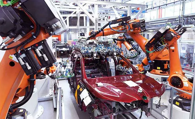
Robots in Automotive Manufacturing Assembly
Automatic Inspection Assembly Line Control PCB Solutions are pivotal to modern manufacturing, enabling unparalleled precision and efficiency across a multitude of industries. These specialized PCBs serve as the intelligent backbone, orchestrating complex inspection routines and robotic assembly processes, thereby ensuring product quality and optimizing operational throughput. Their versatility allows them to be tailored to the unique demands of diverse sectors, from high-volume consumer electronics to safety-critical medical devices and robust automotive components.
Ultra-high precision and reliability, compliance with strict regulatory standards (e.g., ISO 13485), traceability and validation support
Consumer Goods
Appliance assembly inspection, packaging integrity checks, cosmetic defect detection, high-volume product sorting and quality control
Reduced waste and rework, consistent product quality, rapid inspection for fast-moving consumer goods (FMCG), cost efficiency at scale
Aerospace & Defense
Avionics assembly inspection, structural integrity verification, critical component placement in engines and airframes, payload integration
Extreme environmental tolerance, robust performance in harsh conditions, long-term reliability for mission-critical systems, compliance with stringent quality requirements
How do Automatic Inspection Assembly Line Control PCBs enhance quality control in manufacturing? These PCBs integrate advanced sensors and vision systems with high-speed microcontrollers to perform real-time, objective defect detection. By automating inspection, they eliminate human error, consistently apply quality standards, and provide data for process optimization, significantly improving overall product quality and reducing rework or scrap rates compared to manual methods.
Zero One Solution Limited's expertise lies in developing highly adaptable and robust PCB solutions that cater to these specific industrial requirements, driving innovation and efficiency in every sector we serve.
Zero One Solution Limited's Expertise in Action
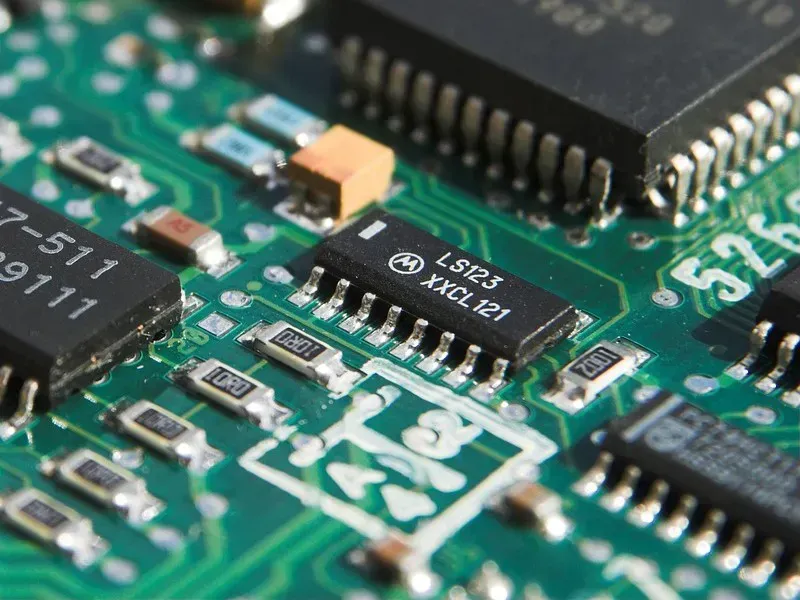
Engineer Designing PCB Circuit Board
At Zero One Solution Limited, our expertise is not just in providing PCBs; it's in delivering a holistic, integrated solution that accelerates product development and ensures the peak performance of Automatic Inspection Assembly Line Control PCBs. With a decade of pioneering innovation since 2011, we have precisely aligned our capabilities with the stringent demands of advanced manufacturing, empowering our clients to bring revolutionary products to market with unparalleled speed and reliability.
Rapid-Response R&D Prototype Manufacturing Our cornerstone capability is rapid prototyping, designed to drastically cut down development cycles. We transform concepts into functional prototypes within days, not weeks, allowing for iterative design improvements and validation crucial for complex automatic inspection systems. This agility ensures that your innovative PCB solutions for automatic inspection are quickly realized and refined.
Comprehensive Design to Assembly Services Zero One Solution offers an end-to-end service model, from initial schematic capture and PCB layout to Design for Manufacturability (DFM) and Design for Assembly (DFA) optimization. Our manufacturing prowess encompasses cutting-edge fabrication techniques for high-density interconnect (HDI) and multi-layer boards, followed by precise assembly, ensuring optimal performance and cost-efficiency for your automatic inspection line control PCBs.
Global Supply Chain and Strategic Locations Headquartered in Shenzhen, China – the global epicenter of electronic manufacturing – and with a strategically vital branch office in Dubai, we harness a robust, global PCBA supply chain. This dual-location strategy ensures seamless access to premium components, efficient logistics, and comprehensive support, guaranteeing timely delivery and competitive pricing for your automatic inspection assembly line control PCB solutions worldwide.
Unwavering Commitment to Client Success Our philosophy revolves around fostering long-term partnerships. We collaborate closely with clients, offering tailored PCB solutions for automatic inspection that directly address their unique challenges and specifications. Our dedicated technical support and quality assurance processes underscore our commitment to not just meeting but exceeding expectations, ensuring your automatic inspection systems achieve optimal operational efficiency and reliability.
Service Aspect
Zero One Solution's Offering
Impact on Automatic Inspection PCB Solutions
Prototyping Speed
Rapid R&D Prototype Manufacturing
Significantly reduces time-to-market for innovative automatic inspection system PCBs.
Design & Engineering
Schematic Capture, Layout, DFM/DFA Optimization
Ensures high reliability and manufacturability of complex control PCBs for inspection lines.
Guarantees robust, high-performance PCBs capable of handling stringent inspection demands.
Supply Chain Advantage
Shenzhen & Dubai Global Network
Optimizes material sourcing and logistics, ensuring cost-effectiveness and timely delivery of automatic inspection PCBs.
Customization
Tailored PCB Solutions
Meets unique requirements for diverse automatic inspection assembly line applications, enhancing system integration.
Future Trends in PCB Design for Automation
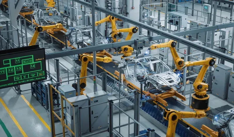
Modern Factory Automation Production Line
The landscape of automatic inspection and assembly lines is continuously evolving, driven by an insatiable demand for efficiency, precision, and adaptability. As a veteran in the PCB solutions industry, Zero One Solution Limited recognizes that the future of these automated systems hinges critically on advancements in PCB design. These future trends will not only refine existing processes but also unlock unprecedented capabilities, allowing for more intelligent, interconnected, and sustainable manufacturing environments. Staying ahead of these technological shifts is paramount to delivering cutting-edge solutions that empower industries to thrive in the era of Industry 4.0 and beyond.
How will Industry 4.0 influence PCB design for automation? Industry 4.0, characterized by the integration of cyber-physical systems, IoT, and AI, demands PCBs capable of robust data processing, secure communication, and real-time decision-making. Future PCB designs will feature enhanced processing power for edge computing, integrated wireless modules for seamless IoT connectivity, and specialized coprocessors for AI/ML algorithms, enabling predictive maintenance and intelligent quality control at the assembly line level. This necessitates multi-layer, HDI, and flex-rigid PCB technologies to accommodate increased component density and complex signal routing, ensuring high performance in dynamic industrial settings.Zero One Solution excels in designing and manufacturing such advanced PCBs, preparing our clients for the demands of smart factories.
What role will edge computing play in future automatic inspection PCBs? Edge computing brings computation and data storage closer to the data sources, significantly reducing latency and bandwidth consumption. For automatic inspection PCBs, this means real-time analysis of sensor data (e.g., from cameras, thermal sensors) directly on the board, enabling immediate defect detection and process adjustments without reliance on cloud-based servers. Future PCB designs will incorporate more powerful embedded processors and dedicated AI accelerators optimized for specific machine vision or anomaly detection tasks, facilitating faster response times and enhancing the autonomy of inspection systems.Zero One Solution is actively integrating powerful edge AI capabilities into our PCB designs, ensuring rapid and localized data processing for critical real-time operations.
How will sustainable manufacturing practices impact PCB design? Sustainable manufacturing emphasizes resource efficiency, waste reduction, and environmental responsibility throughout the product lifecycle. For PCBs, this translates to using eco-friendly materials (e.g., halogen-free laminates, lead-free solders), optimizing power consumption through efficient power management ICs and design techniques, and designing for recyclability and extended product life. The trend also includes modular designs that allow for easy upgrades and repairs, reducing electronic waste.Zero One Solution is committed to sustainable practices, offering design for environment (DFE) considerations and utilizing advanced, environmentally conscious materials and processes in our PCB fabrication.
Zero One Solution Limited stands as your premier partner in navigating the complexities of modern manufacturing automation. Our Automatic Inspection Assembly Line Control PCB Solutions are not just products; they are gateways to enhanced efficiency, unparalleled precision, and significant cost savings. With our rapid prototyping capabilities, global supply chain network, and commitment to excellence, we are uniquely positioned to accelerate your product development and empower your journey towards a fully optimized smart factory. Ready to transform your assembly line with industry-leading PCB technology? Contact Zero One Solution Limited today to discuss how our expertise can drive your innovation forward.