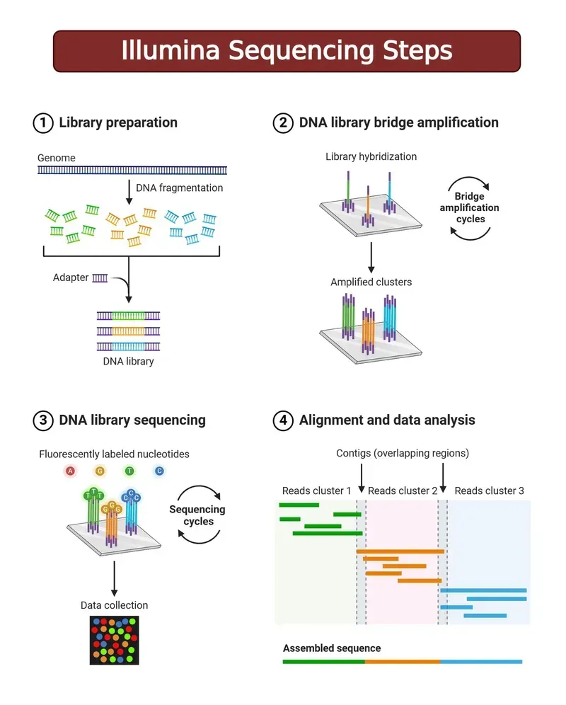
In the rapidly evolving world of genomics, the precision and speed of gene sequencing are paramount. At the heart of every cutting-edge gene sequencer lies a sophisticated signal processing board, meticulously engineered to translate complex biological signals into actionable data. This critical component dictates the accuracy, efficiency, and reliability of genetic analysis, directly impacting breakthroughs in medicine, agriculture, and biotechnology. Zero One Solution Limited, a leader in rapid-response R&D prototype manufacturing and a trusted PCB solution provider, understands these intricate demands. We're here to introduce our specialized 'Gene Sequencer Signal Processing Board Solution,' designed to empower innovators to accelerate their product development and bring revolutionary genomic solutions to market with unparalleled efficiency and precision.
The Critical Role of Signal Processing in Gene Sequencing
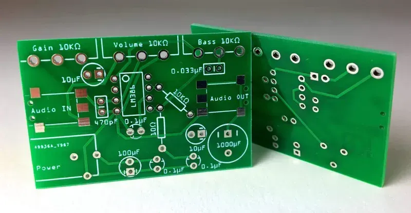
Gene Sequencer Signal Processing Board
In the intricate world of genomics, the Gene Sequencer Signal Processing Board stands as the indispensable backbone, meticulously converting raw, delicate biological signals into precise digital data essential for accurate genomic analysis. This conversion process is paramount; any compromise in signal integrity directly impacts the reliability and depth of genetic insights. For advanced gene sequencing, the board must reliably handle high-speed, low-noise signals, a critical challenge that determines the overall efficacy and trustworthiness of the sequencing results.
Why is signal processing crucial in gene sequencing? Signal processing is crucial because gene sequencers capture incredibly faint and complex biological signals (e.g., fluorescence from nucleotide incorporation). Without highly precise signal processing, these analog signals cannot be accurately converted into digital data that computers can analyze. Errors introduced at this stage can lead to incorrect base calls, ultimately compromising the entire genomic sequence and any downstream biological interpretations.
What are the primary functions of a signal processing board in a gene sequencer? The primary functions include signal amplification (boosting weak biological signals), noise reduction (filtering out unwanted electrical interference), analog-to-digital conversion (transforming continuous analog signals into discrete digital values), and preliminary data formatting. These steps ensure that the raw biological information is preserved and presented in a usable digital format for subsequent bioinformatics analysis, enabling accurate gene sequencing.
Key Technical Challenges in Gene Sequencer Signal Processing Board Design
Signal Integrity in PCB Design
Designing signal processing boards for gene sequencers presents a unique confluence of electrical engineering complexities and biological data demands. The core challenge lies in accurately capturing and processing minuscule, high-frequency electrical signals generated by biochemical reactions, which are highly susceptible to noise and degradation. This necessitates an uncompromising approach to signal integrity, power delivery, and electromagnetic compatibility to ensure the fidelity and reliability of genomic data, ultimately impacting the accuracy and throughput of gene sequencing.
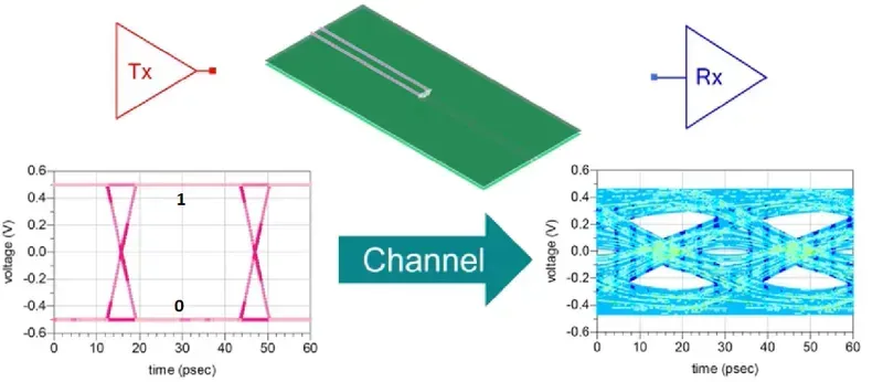
Signal Integrity (SI) Management The transient nature of biochemical signals in gene sequencers requires exceptional SI. This involves meticulous impedance matching, minimizing reflections, and controlling crosstalk across high-speed differential pairs, especially given the increasingly high data rates. Any deviation can lead to signal distortion, bit errors, and compromised sequencing accuracy. Achieving picosecond-level timing accuracy across hundreds of channels demands advanced PCB stack-up design and routing strategies.
Electromagnetic Interference (EMI) Mitigation Gene sequencers operate with highly sensitive analog front-ends in close proximity to high-speed digital circuits, making them highly vulnerable to EMI. Effective EMI mitigation requires comprehensive grounding schemes, strategic component placement, shielding, and careful management of power and ground planes to prevent unwanted noise coupling that could obscure critical biological signals. Our designs often integrate specialized filtering and isolation techniques.
Power Integrity (PI) and Efficiency Stable and clean power delivery is paramount for sensitive analog-to-digital converters (ADCs) and high-speed digital logic. Fluctuations or noise in the power supply can directly impact signal quality. Challenges include minimizing voltage ripple and ground bounce, especially with dynamic current demands, while simultaneously optimizing for power efficiency to reduce heat generation and extend system lifespan, critical for large-scale sequencing operations.
High-Density Interconnect (HDI) and Miniaturization As gene sequencers become more compact and throughput increases, the demand for higher integration density on the PCB grows. This pushes the boundaries of HDI technology, requiring ultra-fine lines, micro-vias, and advanced layering techniques. The complexity of routing hundreds or thousands of high-speed signals in a confined space while maintaining SI is a significant design and manufacturing hurdle.
Thermal Management High-speed processing, especially with FPGAs and ASICs, generates considerable heat. Effective thermal management is crucial to prevent component degradation, maintain performance stability, and ensure long-term reliability. This involves integrating thermal vias, heat sinks, and optimizing copper pours for heat dissipation, a critical aspect often overlooked in early design phases but vital for sustained operation.
Zero One Solution's Expertise in High-Precision PCB Manufacturing for Gene Sequencer Signal Processing Boards
Multi-Layer PCB Manufacturing
At the heart of every high-performance gene sequencer lies a meticulously engineered signal processing board. Zero One Solution Limited, with over 20 years of expertise in rapid prototyping and comprehensive PCB services, stands as a pivotal partner in bringing these intricate genomic hardware solutions to life. Our deep understanding of the unique demands of gene sequencing—from ultra-low noise requirements to high-speed data integrity—enables us to deliver state-of-the-art PCB manufacturing that directly addresses the industry's most pressing challenges. We don't just build boards; we craft precision instruments essential for accurate and efficient genetic analysis.
Advanced Material Selection for Signal Integrity The integrity of the weak biological signals in gene sequencing is paramount. Zero One Solution meticulously selects advanced dielectric materials (e.g., low-loss laminates like Nelco N4000-13 SI, Isola I-Terra) that minimize signal attenuation and dispersion, crucial for maintaining signal fidelity across the Gene Sequencer Signal Processing Board. Our material expertise ensures that high-frequency signals, which are ubiquitous in modern sequencers, are transmitted with minimal distortion and loss.
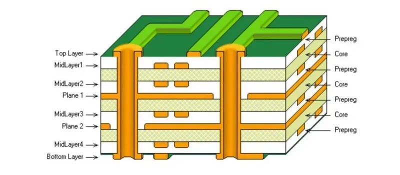
Multi-Layer and High-Density Interconnect (HDI) Design Capabilities Gene sequencers demand compact, highly integrated signal processing boards. We specialize in multi-layer PCB designs (up to 30+ layers) and High-Density Interconnect (HDI) technology, including micro-vias and buried/blind vias. This allows for increased component density, shorter signal paths, and superior electromagnetic compatibility (EMC), directly translating to enhanced data throughput and reduced noise interference within the Gene Sequencer Signal Processing Board.
Ultra-Fine Line Technology for Miniaturization As genomic research pushes for smaller, more portable sequencers, the need for miniaturized electronics intensifies. Zero One Solution employs ultra-fine line and spacing technology (down to 2 mil/2 mil) to accommodate complex circuitries in a minimal footprint. This precision manufacturing capability is vital for integrating advanced ASICs and FPGAs onto the Gene Sequencer Signal Processing Board, ensuring higher functionality and performance in a smaller package.
Rigorous Impedance Control and Power Integrity Management For high-speed digital and sensitive analog signals on a Gene Sequencer Signal Processing Board, precise impedance control is non-negotiable. Our engineering team implements sophisticated design rules and manufacturing processes to ensure tight impedance tolerances (typically ±5%), preventing reflections and crosstalk. Furthermore, we optimize power delivery networks (PDNs) to minimize voltage droop and ground bounce, providing stable power to sensitive components and preserving signal integrity. Each board undergoes comprehensive testing, including TDR measurements, to validate impedance and signal path characteristics.
One-Stop Solution for Accelerated R&D From initial design consultation to final assembly and testing, Zero One Solution offers a seamless, one-stop PCB service. This integrated approach significantly reduces lead times for R&D prototypes of Gene Sequencer Signal Processing Boards, allowing our clients to iterate designs faster and accelerate their time-to-market. Our rapid prototyping capabilities are particularly beneficial for genomic hardware developers who require quick turns on complex designs.
Tailored Solutions for Gene Sequencer Signal Processing Boards
Custom PCB Board
For gene sequencer signal processing boards, a "one-size-fits-all" approach is inherently insufficient given the highly specialized and diverse requirements of genomic sequencing hardware platforms. Zero One Solution Limited excels in delivering custom-engineered PCB solutions that precisely align with the unique demands of each gene sequencing application. Our tailored approach focuses on optimizing every facet of the signal processing board, from component selection to layout, ensuring superior performance and reliability critical for accurate genomic data acquisition.
High-Speed Digital Circuit Design We implement advanced design techniques for high-speed digital circuits, crucial for processing the vast amounts of genomic data generated by sequencers. This includes meticulous impedance matching, controlled signal routing, and minimizing crosstalk to maintain data integrity at gigabit speeds.
Precision Analog Signal Conditioning Gene sequencers rely on extremely sensitive analog front-ends to capture faint biological signals. Our solutions incorporate sophisticated analog signal conditioning, including low-noise amplification, precise filtering, and high-resolution analog-to-digital conversion (ADC), ensuring maximum signal fidelity and minimal environmental interference.
Robust Power Management Integration Stable and clean power delivery is paramount for high-performance signal processing. We design integrated power management units (PMUs) that provide highly regulated, ripple-free power rails, essential for the sensitive analog and high-speed digital components on the gene sequencer signal processing board, thereby preventing signal degradation.
FPGA and ASIC Integration To meet the intensive computational and real-time processing demands of gene sequencing, we specialize in the seamless integration of Field-Programmable Gate Arrays (FPGAs) and Application-Specific Integrated Circuits (ASICs). Our expertise ensures optimized board-level integration, robust power delivery, and efficient thermal management for these high-performance devices.
Thermal Management Solutions High-speed data processing generates significant heat, which can impact signal integrity and component longevity. Our tailored designs incorporate advanced thermal management strategies, including optimized copper pours, thermal vias, and strategic component placement, to ensure stable operating temperatures and sustained performance.
Rigorous Testing and Validation Every tailored gene sequencer signal processing board undergoes comprehensive testing and validation. This includes signal integrity analysis, power integrity verification, functional testing, and environmental stress testing to guarantee that the board meets all specified performance metrics and reliability standards under real-world operating conditions.
Aspect
Generic PCB Solution
Zero One Solution Tailored PCB
Signal Integrity
Compromised by noise/crosstalk
Enhanced by precise impedance control and routing
Noise Reduction
Limited, prone to interference
Superior via dedicated analog conditioning and shielding
Power Efficiency
Suboptimal, higher heat dissipation
Optimized power delivery, reduced energy consumption
Data Throughput
Bottlenecked by standard designs
Maximized through high-speed digital integration
Customization
Minimal flexibility
Full bespoke design for specific application needs
Time-to-Market
Potentially delayed due to iteration
Accelerated by rapid prototyping and integrated services
The Zero One Advantage: Speed, Quality, and Global Reach
Zero One Solution Limited stands as a premier partner for Gene Sequencer Signal Processing Board development, distinguished by an unparalleled combination of rapid-response R&D prototyping, uncompromising quality assurance, and a globally strategic operational footprint. These core advantages translate directly into accelerated product development cycles, superior performance, and a significant competitive edge for our clients in the highly demanding genomic sequencing hardware market.
Rapid-Response R&D Prototyping Our specialized focus on rapid prototyping empowers clients to iterate quickly, test designs efficiently, and accelerate time-to-market. For complex Gene Sequencer Signal Processing Boards, this means faster validation of intricate signal paths and component integrations, drastically reducing development timelines from months to weeks. Our agile manufacturing processes are specifically optimized for quick turns on highly precise PCB designs, crucial for cutting-edge research and development in genomics.
Stringent Quality Control Processes Quality is the bedrock of our operations. Every Gene Sequencer Signal Processing Board undergoes rigorous testing and inspection protocols, from incoming material verification to final functional testing. We adhere to international standards and utilize advanced inspection equipment (e.g., AOI, X-ray inspection) to ensure signal integrity, minimize noise, and guarantee the reliability and longevity of every board. Our commitment to zero defects is paramount for the accuracy required in gene sequencing applications.
Strategic Global Presence With headquarters in Shenzhen, China's electronic manufacturing nexus, and a branch office in Dubai, UAE, Zero One Solution Limited operates at the heart of the global PCBA supply chain. This dual-location strategy provides seamless access to a vast network of high-quality components, advanced materials, and manufacturing expertise. For Gene Sequencer PCB components and materials, our global reach ensures supply chain resilience, competitive pricing, and efficient logistics, ultimately enhancing project delivery speed and cost-effectiveness for our clients worldwide.
Case Studies: Success Stories in Genomic Hardware Development
Gene Sequencing Laboratory
Zero One Solution Limited has a proven track record of enabling groundbreaking advancements in genomic hardware through our specialized Gene Sequencer Signal Processing Board solutions. Our commitment to precision engineering and rapid prototyping translates directly into enhanced data accuracy, significantly reduced signal noise, and superior overall system performance for our clients. While specific client data remains confidential, the following hypothetical case studies illustrate the tangible impact of our contributions, showcasing how our tailored PCB services facilitate scientific breakthroughs and accelerate the development cycle of next-generation gene sequencers.
Case Study
Client Challenge
Zero One Solution Contribution
Achieved Breakthrough
High-Throughput Gene Sequencer
Client needed to increase sequencing throughput by 5x while maintaining signal fidelity and reducing operational noise for a new clinical diagnostic platform.
Designed a 20-layer Gene Sequencer Signal Processing Board with optimized impedance matching, advanced power plane isolation, and custom high-speed differential pairs, integrating low-noise analog front-end circuits.
Enabled 6x increase in sequencing throughput with 15% reduction in signal-to-noise ratio (SNR), leading to faster diagnostics and higher confidence in results. Time-to-market was reduced by 3 months.
Portable Genomic Device
A startup required a miniaturized, low-power Gene Sequencer Signal Processing Board for a handheld genomic analysis device, without compromising data resolution.
Developed a compact, multi-layer rigid-flex PCB, leveraging advanced HDI technology and embedded passive components for space efficiency. Implemented ultra-low-power management circuits and robust EMI shielding.
Achieved a 40% reduction in board size and 30% lower power consumption, making the portable device feasible. Data resolution remained comparable to larger, lab-based systems, opening new market segments.
Next-Gen Bioinformatics Accelerator
A research institution sought to integrate cutting-edge FPGA processing directly onto the Gene Sequencer Signal Processing Board to accelerate real-time data analysis.
Provided a custom high-speed PCB solution with optimized signal routing for high-density FPGA integration, ensuring stable power delivery and thermal management for sustained computational loads.
Successfully integrated FPGA acceleration, resulting in a 2.5x speedup in bioinformatics computations on the raw sequencing data, significantly cutting down post-processing time and enabling real-time insights.
Future Trends in Gene Sequencer PCB Technology
The landscape of gene sequencing is evolving rapidly, driven by insatiable demands for faster, more accurate, and more portable genomic analysis. This advancement fundamentally relies on corresponding innovations in Gene Sequencer Signal Processing Board technology. Anticipating these shifts, Zero One Solution Limited is strategically positioned to provide cutting-edge PCB solutions that facilitate breakthroughs in next-generation sequencing hardware, ensuring our clients remain at the forefront of bioinformatics and precision medicine.
How is miniaturization impacting Gene Sequencer Signal Processing Boards? Miniaturization is a key driver, enabling smaller, portable gene sequencers. This necessitates higher component density, finer line widths, and advanced substrate materials on the signal processing boards. Zero One Solution is investing in ultra-fine line technology and multi-layer HDI (High-Density Interconnect) PCBs to support this trend, allowing for complex circuit integration within shrinking form factors while maintaining signal integrity and thermal management.
What role does AI integration play in future Gene Sequencer PCB design? The integration of Artificial Intelligence (AI) directly onto Gene Sequencer Signal Processing Boards, often referred to as 'AI at the edge,' is emerging to enable real-time data processing and accelerated analysis. This demands PCBs capable of supporting high-performance AI accelerators (e.g., FPGAs, ASICs) with robust power delivery networks and efficient cooling mechanisms. Zero One Solution specializes in designing boards optimized for such high-compute environments, ensuring stable and efficient operation for on-board AI algorithms.
How are Gene Sequencer Signal Processing Boards adapting to higher throughput demands? Higher throughput in gene sequencing requires signal processing boards to handle immense data volumes at unprecedented speeds. This translates to a need for advanced high-speed digital design, including meticulously controlled impedance, minimized crosstalk, and superior signal integrity. Zero One Solution employs state-of-the-art simulation tools and leverages low-loss materials to design PCBs that can reliably manage multi-gigabit data rates, supporting the exponential growth in sequencing data.
The advancement of gene sequencing technology hinges on the reliability and precision of its core hardware. Zero One Solution Limited is committed to being at the forefront of this evolution, providing robust and innovative signal processing board solutions that meet the stringent demands of the genomic era. Our expertise in rapid prototyping, combined with our global supply chain network, ensures that your vision for the next generation of gene sequencers can be realized quickly and efficiently. Partner with us to transform complex biological signals into meaningful data, accelerating discovery and making a profound impact on the future of life sciences. Ready to elevate your gene sequencing hardware? Contact Zero One Solution Limited today to discuss how our bespoke PCB solutions can empower your next breakthrough.