In the rapidly evolving landscape of wireless communication, base stations form the backbone of connectivity, demanding unparalleled performance from every component. At the heart of a base station's ability to transmit and receive signals efficiently lies its RF (Radio Frequency) Front-end, and crucially, the Printed Circuit Board (PCB) that underpins it. The design and manufacturing of these PCBs are critical to ensuring high-frequency signal integrity, power efficiency, and overall system reliability. Zero One Solution Limited, a leader in rapid prototyping and one-stop PCB solutions, understands these complex demands. This article delves into the intricacies of Base Station RF Front-end PCB solutions, showcasing how our expertise empowers telecommunications innovators to build the next generation of wireless infrastructure.
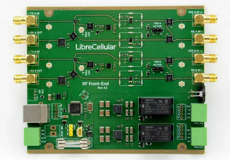
At the heart of every high-performance base station, the Radio Frequency (RF) Front-end Printed Circuit Board (PCB) serves as the foundational element, dictating the overall system efficiency, signal quality, and reliability. This critical component is responsible for processing the intricate high-frequency signals that enable wireless communication, making its design and manufacturing paramount for optimal performance in modern wireless networks, especially with the demanding requirements of 5G infrastructure. A well-engineered RF front-end PCB ensures minimal signal loss, excellent impedance matching, and robust electromagnetic compatibility, directly impacting a base station's ability to transmit and receive data with precision and efficiency.
| Network Generation | Key Frequency Bands | Impact on RF Front-end PCB |
|---|---|---|
| 4G LTE | 700 MHz - 2.6 GHz | Focus on lower loss, reliable signal paths, and power efficiency across multiple bands. Challenges include interference mitigation and compact designs for urban deployments. |
| 5G New Radio (NR) - Sub-6 GHz | 600 MHz - 7.125 GHz | Increased bandwidth and higher data rates demand tighter impedance control and superior signal integrity. Support for Massive MIMO requires more complex, multi-layered PCBs with advanced routing capabilities and thermal management for denser component integration. |
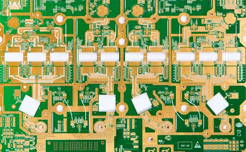
Designing PCBs for Base Station RF Front-ends presents a multifaceted engineering challenge, demanding precision to ensure optimal signal transmission and reception in high-frequency wireless networks. The core complexity lies in managing critical electromagnetic behaviors that directly impact network performance, from signal integrity and power efficiency to thermal stability and noise suppression. Successfully navigating these hurdles is paramount for delivering robust, high-performance base station infrastructure capable of supporting advanced communication protocols like 5G and beyond.
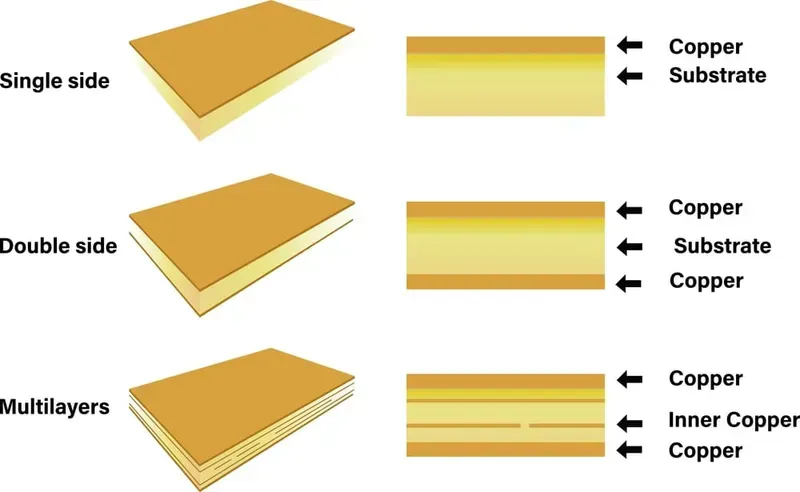
The performance of Base Station RF Front-end PCBs at high frequencies is fundamentally determined by the advanced materials chosen for their construction. These specialized substrates are engineered to minimize signal loss, maintain impedance control, and ensure thermal stability, which are critical for the robust operation of base station RF front-end modules and overall 5G infrastructure. Selecting the right material is paramount to achieving superior signal integrity and reliability in demanding wireless communication environments.
| Material Type | Key Characteristics | Typical Application in RF PCBs | Advantages | Disadvantages |
|---|---|---|---|---|
| Low-Loss Laminates (e.g., Rogers, Arlon) | Excellent dielectric constant (Dk) stability, low dissipation factor (Df) | Antenna arrays, power amplifiers, filters | Superior signal integrity, reduced insertion loss, high frequency performance | Higher cost, more specialized fabrication processes |
| Ceramic-Filled Hydrocarbons (e.g., Duroid series) | Extremely low Dk and Df, high thermal conductivity, mechanical stability | High-power RF circuits, millimeter-wave applications | Exceptional electrical performance at very high frequencies, good heat dissipation | Higher material cost, can be brittle |
| PTFE (Polytetrafluoroethylene) Composites | Very low Dk and Df, wide operating temperature range, chemical inertness | Phased array antennas, aerospace and defense RF systems | Excellent performance in harsh environments, low signal distortion | Poor dimensional stability, difficult to process |
| Modified Epoxy Resins (e.g., enhanced FR-4) | Improved Dk/Df compared to standard FR-4, cost-effective | Intermediate frequency applications, less demanding RF front-ends | Lower cost, widely available, easier to process | Performance limitations at very high frequencies, higher loss than specialty materials |
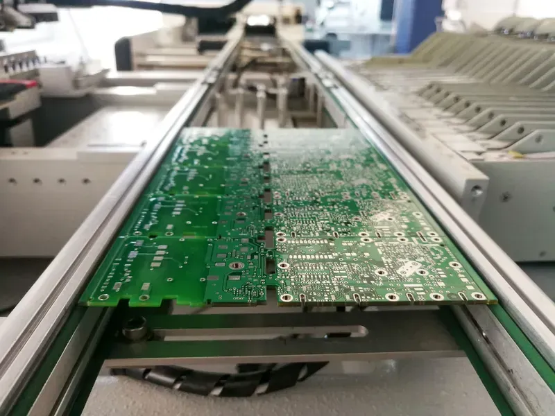
Zero One Solution Limited offers a holistic suite of PCB solutions specifically engineered to meet the demanding requirements of base station RF front-end applications. From initial concept and intricate design to rapid prototyping, precision manufacturing, and final assembly, our integrated approach ensures seamless development and delivery of high-performance PCBs critical for robust wireless infrastructure.
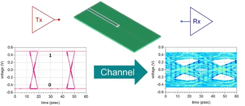
In the demanding landscape of modern wireless infrastructure, the unwavering signal integrity and long-term reliability of Base Station RF Front-end PCBs are not merely desirable – they are absolutely critical. Any degradation in signal quality or system uptime directly impacts network performance, user experience, and operator profitability. Zero One Solution Limited stands at the forefront of this challenge, employing a comprehensive suite of advanced design techniques and rigorous testing procedures to meticulously engineer PCBs that guarantee superior signal purity, minimize loss, and ensure robust, unfailing operation throughout their lifecycle.
Achieving pristine signal integrity in high-frequency RF front-ends demands a multi-faceted design approach. Precise impedance matching, typically to 50 ohms, is paramount to prevent signal reflections and maximize power transfer. Zero One Solution Limited employs sophisticated simulation tools and controlled impedance routing methodologies, including careful trace width, spacing, and dielectric constant management within the PCB stack-up. Furthermore, minimizing electromagnetic interference (EMI) and crosstalk between high-speed signal lines is crucial. This is addressed through optimal component placement, strategic grounding schemes, and the intelligent use of guard traces and shielding, all meticulously designed to maintain signal isolation.
Beyond signal propagation, power integrity (PI) is fundamental. Stable and clean power delivery to sensitive RF components is ensured through robust power distribution networks (PDNs), effective decoupling capacitor strategies, and optimized power and ground planes to suppress noise and voltage ripple. Thermal management also plays a critical role, as high-frequency RF components generate heat that can degrade performance and reliability. We implement advanced thermal management solutions such as optimized copper pours, thermal vias, and careful consideration for heat sink integration to maintain stable operating temperatures and extend component lifespan.
To validate these designs and guarantee long-term reliability, Zero One Solution Limited implements rigorous testing procedures. Our validation processes include comprehensive S-parameter measurements using vector network analyzers (VNAs) to characterize insertion loss, return loss, and isolation across the operational frequency spectrum. Time Domain Reflectometry (TDR) is precisely utilized for impedance profiling and accurate fault location. Beyond electrical performance, long-term reliability is assured through rigorous environmental testing, including thermal cycling, humidity exposure, and vibration tests, simulating harsh operating conditions to guarantee the PCB's durability and consistent performance over time. Every PCB undergoes stringent manufacturing quality checks, including Automated Optical Inspection (AOI), X-ray inspection for internal layers, and flying probe or bed-of-nails testing to verify connectivity and identify any manufacturing defects, ensuring the delivery of mission-critical components for robust wireless infrastructure.
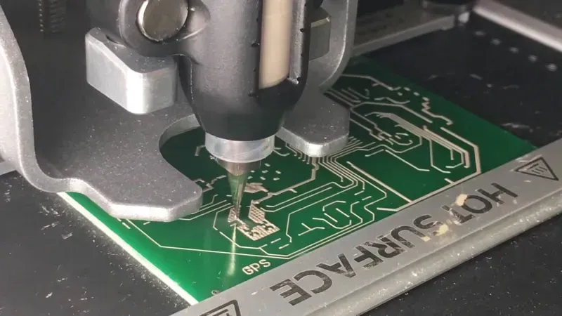
In the fast-evolving landscape of wireless communication, particularly with the advent of 5G and beyond, the ability to rapidly iterate and validate new base station technologies is paramount. Zero One Solution Limited's rapid prototyping services are specifically engineered to significantly reduce the time-to-market for complex RF front-end PCB designs, providing a critical competitive edge. This agile approach empowers our clients to quickly transform innovative concepts into tangible, testable prototypes, ensuring efficient validation and accelerated product development cycles.
Zero One Solution Limited's commitment to rapid prototyping is a testament to our dedication to accelerating our clients' innovation pipelines. By providing a swift, reliable, and cost-effective pathway from concept to validated prototype, we empower our partners to stay ahead in the fiercely competitive telecommunications market.
The evolution of wireless communication demands increasingly sophisticated Base Station RF Front-end PCB technology. As 5G deployment accelerates and 6G research begins, future trends in base station RF front-end PCB design will be characterized by a relentless pursuit of higher frequencies, greater integration, and enhanced power efficiency. Zero One Solution Limited is at the forefront of these advancements, anticipating and adapting to these shifts to provide cutting-edge PCB solutions that meet the stringent demands of next-generation wireless infrastructure.
| Future Trend | Impact on PCB Design | Zero One Solution Limited's Approach |
|---|---|---|
| Higher Frequencies (mmWave) | Ultra-low loss materials, precise impedance control, minimal signal attenuation | Utilization of advanced RF laminates (e.g., PTFE, ceramic-filled hydrocarbons), rigorous DFM for high-frequency routing |
| Massive MIMO & Beamforming | High component density, complex multi-layer routing, thermal management for increased power | Expertise in HDI, multi-layer designs, advanced thermal vias, and material selection for heat dissipation |
| Enhanced Power Efficiency | Integration of GaN/GaAs components, efficient power delivery networks (PDN) | Optimized PDN design, specialized materials for high power handling, robust thermal management solutions |
| Integrated Solutions (SoP) | Miniaturization, reduced parasitics, potential for 3D packaging | Advanced packaging techniques, embedded component capabilities, rapid prototyping for complex module validation |
Navigating the complexities of Base Station RF Front-end PCB Solutions requires in-depth knowledge and precise execution. This section addresses common inquiries about the design, manufacturing, and performance of PCBs critical for base station RF front-ends, offering practical insights and expert answers to help clients understand the intricate challenges and effective solutions in this specialized field.
| Feature | Impact on RF Front-end PCB | Importance for Base Stations |
|---|---|---|
| Low-Loss Materials | Minimizes signal attenuation at high frequencies | Crucial for maintaining signal strength and range, especially in 5G |
| Precise Impedance Control | Ensures maximum power transfer and minimal signal reflection | Vital for stable RF performance and preventing standing waves |
| Thermal Management | Dissipates heat from power components | Prevents performance degradation and extends component lifespan in high-power applications |
| EMI Shielding | Reduces external noise and prevents internal interference | Ensures clean signal reception and transmission in crowded RF environments |
The demands placed on Base Station RF Front-end PCBs are ever-increasing, driven by the relentless pursuit of faster, more reliable, and more efficient wireless communication. From managing high-frequency signals and heat dissipation to ensuring precise impedance matching and robust reliability, the challenges are significant. Zero One Solution Limited stands as your strategic partner in navigating these complexities. With our proven expertise in rapid prototyping, design optimization, and advanced manufacturing capabilities, we empower our clients to accelerate their product development cycles and bring groundbreaking base station technologies to market with confidence. Partner with Zero One Solution Limited and let's build the future of connectivity together. Visit our website or contact us today to discuss how our bespoke PCB solutions can elevate your next base station project.

