In the dynamic and demanding landscape of modern warfare, real-time situational awareness is paramount. Battlefield sensor networks, the silent sentinels of the digital age, are pivotal in achieving this critical advantage. At the heart of these indispensable systems lies the Printed Circuit Board (PCB) – the foundational technology dictating performance, reliability, and resilience. As a veteran engineer from Zero One Solution Limited, I've witnessed firsthand the rigorous demands placed on electronic components in theater. This article delves into the specialized PCB solutions essential for designing and deploying robust, high-performance battlefield sensor network nodes, outlining how Zero One Solution Limited, with our rapid prototyping and one-stop service from design to assembly, empowers defense innovators to bring their critical systems to market with unparalleled efficiency.
The Strategic Importance of Battlefield Sensor Networks
In modern military operations, Battlefield Sensor Networks (BSNs) are indispensable, serving as the digital eyes and ears on the ground to provide real-time intelligence, surveillance, and reconnaissance (ISR) capabilities. The unwavering reliability of these networks is paramount for mission success, directly influencing tactical decisions, force protection, and operational effectiveness. At the very core of each sensor node, the Printed Circuit Board (PCB) acts as the foundational backbone, orchestrating every critical function. Consequently, robust and meticulously engineered Battlefield Sensor Network Node PCB Solutions are not merely components but strategic assets that dictate the survivability and performance of these vital systems in the most demanding environments.
Strategic Benefit
Impact on Military Operations
Role of PCB Solution
Enhanced Situational Awareness
Provides commanders with a comprehensive, real-time understanding of the battlespace, enabling quicker, more informed decisions.
Integrates various sensors (acoustic, seismic, thermal) and communication modules seamlessly, ensuring accurate data acquisition and transmission.
Improved Intelligence Gathering
Collects critical data on enemy movements, activity patterns, and environmental conditions without direct human exposure.
Houses advanced processing units and secure data encryption hardware, enabling efficient, reliable, and secure data handling from source to analysis.
Force Protection & Early Warning
Detects potential threats (e.g., troop movements, vehicle presence) at a distance, providing crucial time for defensive actions.
Ensures the resilience and low-power operation of detection circuits, enabling long-duration surveillance with minimal maintenance in hostile terrains.
Targeting & Strike Coordination
Facilitates precise targeting by providing accurate location and identification of high-value assets.
Supports high-frequency signal integrity and robust power delivery for communication systems critical for synchronized strike operations.
Logistics & Resource Optimization
Monitors supply lines, equipment status, and environmental factors to optimize resource deployment and reduce operational costs.
Designed for ruggedness and extended operational life, minimizing failure rates and reducing the logistical burden of frequent replacements or repairs.
Key Design Considerations for Battlefield Sensor Network Node PCBs
Military PCB Board Design for Harsh Environments
Designing Printed Circuit Boards (PCBs) for battlefield sensor network nodes demands a rigorous approach, far exceeding commercial standards. The core challenge lies in engineering a board that can not only function flawlessly but also endure and perform optimally under the most extreme and unpredictable military operational environments. These specialized PCBs are the technological backbone ensuring uninterrupted data collection and transmission, directly impacting mission success and personnel safety. Therefore, every design choice, from component selection to layout, must prioritize resilience, reliability, and precision to meet the formidable requirements of the modern battlefield.
Extreme Environmental Resistance Battlefield sensor nodes are exposed to severe conditions. PCBs must be designed to withstand extreme temperature fluctuations (from sub-zero to scorching deserts), high humidity, dust, sand, and chemical exposure (e.g., fuels, lubricants). This necessitates selecting materials with stable thermal properties and applying robust conformal coatings to prevent ingress and corrosion. For example, operational temperatures can range from -40
G0C to +85
G0C, requiring components rated for these extremes and thermal management solutions like heat sinks or specialized thermal vias.
Shock and Vibration Durability Military applications involve constant movement, impacts, and explosions. PCBs for battlefield sensor nodes must be engineered to resist significant mechanical shock (e.g., up to 100g for 6ms) and continuous vibration (e.g., 20-2000 Hz at 10-20g RMS). This typically involves using thicker copper traces, robust component mounting (e.g., staking, underfill), and rigid-flex or specialized substrates that absorb mechanical stress, ensuring solder joint integrity and preventing component detachment under dynamic loads. Adherence to MIL-STD-810G standards for shock and vibration is paramount.
Design Consideration
Impact on Battlefield Sensor Node Performance
Zero One Solution Limited Approach
EMI/EMC Shielding
Prevents interference from external electromagnetic sources and limits emissions from the node itself, crucial for stealth and reliable communication.
Utilizes multi-layer stack-ups with ground planes, differential pair routing, and strategic component placement to minimize EMI, adhering to MIL-STD-461 for electromagnetic compatibility and employing specialized shielding materials for critical circuits. Ensures signal integrity even in contested electromagnetic environments.
Size, Weight, and Power (SWaP) Optimization For deployable battlefield sensors, every gram and cubic centimeter matters. PCBs must be compact and lightweight, utilizing high-density interconnect (HDI) technologies and miniaturized components. Power efficiency is equally critical to extend battery life, requiring careful selection of low-power components, efficient power management ICs, and optimized circuit designs. Reducing SWaP directly translates to increased operational range and reduced logistical burden for troops in the field, with power consumption often targeted in the microwatt range during standby and low-milliwatt during active operation.
Material Selection for Extreme Environments
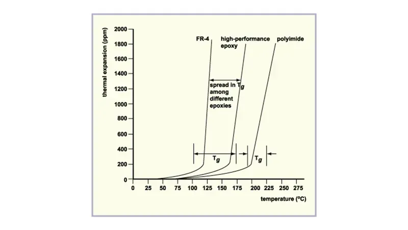
High-Tg Laminate Material for PCBs
For battlefield sensor network nodes, the selection of PCB materials is paramount, directly influencing their resilience and operational longevity in unforgiving environments. Beyond standard considerations, military-grade applications demand materials that exhibit superior thermal stability, optimal dielectric performance for high-frequency data transmission, and unwavering resistance to environmental stressors such as moisture, chemicals, and mechanical shock. This meticulous material engineering ensures the PCB, the backbone of the sensor node, maintains integrity and functionality amidst the most extreme conditions encountered on the modern battlefield.
Excellent thermal stability, high glass transition temperature (Tg), good mechanical strength, cost-effective.
Foundation for rigid PCBs in standard operating temperatures, resisting delamination under thermal stress from components or environmental heat spikes. Ideal for processing units and power sections where heat generation is significant.
Superior thermal conductivity, high-frequency performance, excellent dimensional stability, chemical inertness, high strength.
High-power RF modules, microwave circuits, and sensor elements requiring precise impedance control and efficient heat dissipation. Enables robust operation in extreme temperatures and corrosive environments.
Material Type
Key Properties for Battlefield Use
Applications in Battlefield Sensor Nodes
Flexible and Rigid-Flex Materials (e.g., Polyimide, LCP)
High flexibility, space-saving, shock and vibration resistance, lightweight, good electrical performance.
Connecting modules in compact enclosures, wearable sensors, and systems requiring dynamic movement or complex 3D integration. Enhances durability against battlefield shocks and vibrations.
Material Type
Key Properties for Battlefield Use
Applications in Battlefield Sensor Nodes
Low Loss / High-Frequency Laminates (e.g., PTFE, Hydrocarbon Ceramics)
Low dielectric loss tangent, stable dielectric constant over frequency and temperature, excellent signal integrity.
Crucial for high-speed data transmission, antenna arrays, and RF communication modules in sensor nodes, ensuring accurate and reliable signal propagation for critical intelligence.
Advanced Manufacturing and Assembly Techniques for Battlefield Sensor Network Node PCBs
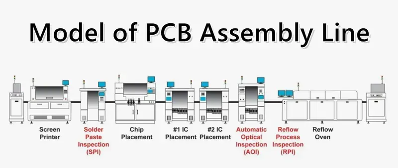
PCB Circuit Board Assembly Line
The unparalleled demands of battlefield environments necessitate highly specialized manufacturing and assembly techniques for sensor network node PCBs, far exceeding commercial standards. These advanced processes ensure that critical components withstand extreme conditions, maintain integrity, and perform flawlessly when reliability is paramount. Precision in every stage, from material handling to final assembly, is critical to producing robust, high-performance battlefield sensor network node PCBs.
IPC Class 2/3 Standards Compliance Military-grade PCBs, especially for battlefield sensor network nodes, must adhere to stringent IPC Class 2 (Dedicated Service Electronic Products) or, more commonly, Class 3 (High-Reliability Electronic Products) standards. These define rigorous requirements for material quality, soldering integrity, cleanliness, and overall workmanship, ensuring maximum operational reliability under stress. Adherence to these standards is non-negotiable for mission-critical applications.
Conformal Coating Application Conformal coatings are thin, protective polymer films applied to PCB assemblies to protect the electronic circuits from environmental stresses such as moisture, dust, chemical contaminants, and extreme temperatures. For battlefield sensor network nodes, various coating types (acrylic, silicone, urethane, parylene) are selected based on specific environmental threats and required dielectric properties, significantly enhancing durability and extending operational life.
Potting and Encapsulation Potting involves enclosing the entire PCB assembly or specific sensitive components within a resin compound, providing superior protection against shock, vibration, moisture, and tampering. This technique is particularly vital for battlefield sensor nodes to withstand ballistic impact, harsh weather, and ensure physical security, effectively creating a monolithic, highly durable unit impervious to external threats.
Advanced Soldering Techniques Achieving reliable electrical connections and mechanical integrity in military-grade PCBs requires advanced soldering techniques. This includes lead-free soldering processes compliant with RoHS where applicable, but more critically, highly controlled reflow profiles for surface-mount technology (SMT) components, selective soldering for through-hole components, and meticulous inspection (e.g., X-ray) to detect voids or defects. Precision soldering minimizes points of failure in dynamic battlefield conditions.
Stringent Quality Control and Testing Beyond visual inspection, battlefield sensor network node PCBs undergo extensive quality control and testing. This includes Automated Optical Inspection (AOI) for component placement and solder joint quality, In-Circuit Testing (ICT) to verify electrical functionality, and Functional Testing (FCT) to simulate operational conditions. Thermal cycling, vibration testing, and Highly Accelerated Life Testing (HALT) are also crucial to validate performance and longevity under anticipated battlefield stresses.
Power Management and Energy Efficiency in Battlefield Nodes
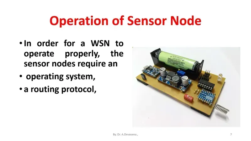
Engineer Operating Battlefield Sensor Node
Effective power management and superior energy efficiency are paramount for battlefield sensor network nodes, directly dictating their operational longevity and mission effectiveness in extended field deployments. Given that these nodes often rely on limited battery power in remote, austere environments, optimizing every watt consumed and exploring self-sustaining power solutions are critical design imperatives for a robust battlefield sensor network node PCB solution. This focus ensures sustained vigilance, reduces the logistical burden of battery resupply, and minimizes the risk of operational downtime, making advanced power strategies a cornerstone of their design.
What are the primary power challenges for battlefield sensor network nodes? Battlefield sensor nodes face significant power challenges, primarily due to their remote deployment, reliance on finite battery power, and the need for continuous operation. Key issues include limited energy reserves, the necessity for ultra-low power consumption in dormant and active states, extreme temperature impacts on battery performance, and the logistical difficulties of resupplying or recharging in hostile environments. Efficient power management for battlefield sensor network nodes directly addresses these constraints.
How does PCB design influence energy efficiency in battlefield sensor network nodes? PCB design profoundly impacts energy efficiency. Strategic layout minimizes trace resistance and capacitance, reducing power loss. Component placement optimizes signal paths, lowering switching losses. Integration of power management ICs (PMICs), voltage regulators with high conversion efficiency, and careful selection of low-power components are crucial. Furthermore, multi-layer PCBs can enable dedicated power planes for stable power delivery, essential for the reliability of battlefield sensor network node PCB solutions.
What strategies can extend the operational life of battery-powered battlefield sensor nodes? Extending operational life involves several strategies: implementing aggressive power cycling and sleep modes, optimizing sensor duty cycles, using energy-efficient microcontrollers and transceivers, and leveraging advanced battery chemistries (e.g., Li-ion, solid-state) with high energy density. Integrating energy harvesting techniques such as solar, kinetic, or thermal energy scavenging can also provide supplementary power, significantly prolonging the field deployment of battlefield sensor network nodes.
Are there specific power delivery network (PDN) considerations for battlefield sensor node PCBs? Absolutely. A robust Power Delivery Network (PDN) on the PCB is vital for battlefield sensor network nodes. This includes wide power and ground planes to minimize impedance, strategic placement of decoupling capacitors to filter noise and stabilize voltage rails, and careful routing to avoid ground bounce and IR drop. Ensuring a stable and clean power supply is critical for the reliable operation of sensitive digital and RF components, particularly under dynamic load conditions common in sensor applications.
How does Zero One Solution Limited address power management in ruggedized PCB solutions for battlefield applications? Zero One Solution Limited leverages its expertise in high-reliability PCB manufacturing and assembly to support advanced power management designs for battlefield applications. We assist in optimizing PCB stack-ups for efficient PDNs, recommend and integrate high-efficiency PMICs, and implement design-for-low-power principles from schematic capture to layout. Our rapid prototyping and precise assembly capabilities ensure that energy-efficient and robust battlefield sensor network node PCB solutions are brought to market swiftly and reliably, enabling extended field operations.
Security and Tamper Resistance Features for Battlefield Sensor Network Node PCBs
Encrypted Chip on PCB
In the volatile theater of battlefield operations, the security and integrity of sensor network nodes are paramount. Beyond their functional capabilities, these critical assets must incorporate robust physical and cyber security features directly into their PCB design to safeguard sensitive intelligence, prevent unauthorized access, and resist reverse engineering. This integrated approach ensures the confidentiality, integrity, and availability of data, making security an indispensable design criterion for every battlefield sensor network node PCB.
Why is PCB-level security crucial for battlefield sensor network nodes? PCB-level security is the foundational layer of defense for battlefield sensor network nodes. It prevents adversaries from physically tampering with the hardware, extracting sensitive data, or injecting malicious code. Without it, even the most sophisticated software-level security can be compromised, as physical access allows for direct manipulation or data extraction from the core components. Integrating security directly into the PCB design ensures a hardware root of trust, making it significantly harder to bypass.
What are common physical tamper resistance mechanisms for battlefield sensor network node PCBs? Physical tamper resistance mechanisms for battlefield sensor network node PCBs include epoxy potting or conformal coating to obscure and protect components, anti-tamper meshes or layers that trigger data erasure upon intrusion, and secure enclosures designed to resist forced entry. Additionally, the strategic placement of critical components and the use of specialized, hard-to-access packages deter physical manipulation and reverse engineering attempts. These measures aim to render the device inoperable or delete sensitive data if unauthorized physical access is detected.
How do secure elements contribute to the security of battlefield sensor network nodes? Secure elements (SEs) are dedicated, tamper-resistant hardware components integrated onto the PCB that provide a secure environment for cryptographic operations, key storage, and secure boot processes. For battlefield sensor network nodes, SEs are vital for generating and protecting encryption keys, authenticating communications, and ensuring the integrity of firmware. They act as a fortress for sensitive information, isolated from the main processor, making it exceedingly difficult for adversaries to compromise the node's cryptographic functions or impersonate legitimate devices.
What role does hardware-based data encryption play in battlefield sensor network nodes? Hardware-based data encryption involves dedicated cryptographic accelerators embedded directly into the PCB's chipset or as standalone modules. This approach offers superior performance and security compared to software-only encryption. For battlefield sensor network nodes, it ensures that all data – whether at rest (stored on memory) or in transit (over the network) – is encrypted efficiently and robustly, protecting critical intelligence from interception and decryption by unauthorized entities. This offloads cryptographic tasks from the main CPU, enhancing both security and energy efficiency.
Zero One Solution Limited: Your Partner in Ruggedized PCB Solutions
In the demanding theatre of battlefield sensor networks, where every component must perform flawlessly under duress, Zero One Solution Limited stands as a proven leader in providing ruggedized PCB solutions. Our decade-long expertise, combined with a relentless focus on rapid prototyping and stringent quality control, ensures that your critical sensor nodes are built on a foundation of uncompromised reliability and performance, directly contributing to mission success and operational superiority.
At Zero One Solution Limited, we understand the unique challenges of military-grade electronics. Our comprehensive capabilities span the entire PCB lifecycle, from initial design consultation to advanced manufacturing and assembly, all tailored to meet the exacting standards of battlefield deployment. We pride ourselves on being a true "one-stop solution" provider, streamlining your development process and accelerating time-to-market for even the most complex projects.
Rapid Prototyping for Accelerated Development Our rapid prototyping services are designed to significantly reduce your development cycles. We can quickly iterate on designs, allowing for swift testing and validation of new sensor node concepts, which is crucial in fast-paced defense technology environments. This agility ensures that your innovations can move from concept to deployment with unprecedented speed and efficiency, giving you a competitive edge.
Service Area
Zero One Solution Limited's Advantage
Impact on Battlefield Sensor Nodes
PCB Design & Layout
Expertise in SWaP optimization, EMI/EMC, and thermal management for extreme conditions.
Enhances sensor node efficiency, reliability, and extends operational lifespan in the field.
Material Sourcing
Global network ensures access to specialized, high-performance military-grade laminates and components.
Guarantees resilience against extreme temperatures, shock, and vibration, crucial for survivability.
Advanced Manufacturing
IPC Class 2/3 standards, conformal coating, potting, and precise assembly processes.
Ensures exceptional durability, integrity, and consistent performance under combat conditions.
Quality Control
Rigorous testing protocols including AOI, X-ray, ICT, and functional testing.
Minimizes field failures, maximizes uptime, and maintains data integrity for critical missions.
Global Supply Chain
Strategic locations in Shenzhen and Dubai provide seamless access to worldwide resources and support.
Enables fast turnaround times and reliable delivery of large-scale production or urgent prototypes.
Why Choose Zero One Solution Limited for Your Battlefield Sensor Network Node PCBs? With a proven track record since 2011, Zero One Solution Limited offers unparalleled experience in complex, high-reliability PCB manufacturing. Our integrated approach ensures consistent quality and seamless project management from concept to completion. We combine Silicon Valley's innovative spirit with Shenzhen's manufacturing prowess, providing a unique blend of cutting-edge technology and cost-effectiveness. Our commitment to ISO 9001 and military standards ensures every PCB meets the most stringent performance criteria. Partner with us to transform your advanced sensor network concepts into resilient, deployable realities that deliver critical intelligence when and where it's needed most.
The operational success of battlefield sensor networks hinges on the unwavering reliability and advanced performance of their underlying PCB technology. As we've explored, the challenges are significant, but with a specialized approach to design, material selection, and manufacturing, these hurdles are surmountable. Zero One Solution Limited stands as your strategic partner in this critical endeavor. With our decade-plus of expertise in rapid-response R&D prototype manufacturing, comprehensive one-stop services, and a global supply chain network, we are uniquely positioned to transform your innovative concepts into field-ready, ruggedized PCB solutions for the most demanding environments. Don't let PCB complexity be a bottleneck in your mission-critical projects. Contact Zero One Solution Limited today to discuss how our expertise can accelerate your battlefield sensor network node development and enhance national security through superior electronic solutions.