From the radios of yesteryear to the microchips of today, bipolar transistors have played a crucial yet often unseen role. These three-terminal semiconductor devices, using both electrons and holes for current flow, are the backbone of countless electronic systems. This article will delve into their operation, types, and applications, uncovering the magic behind these foundational devices and showing their continued relevance in modern technology.
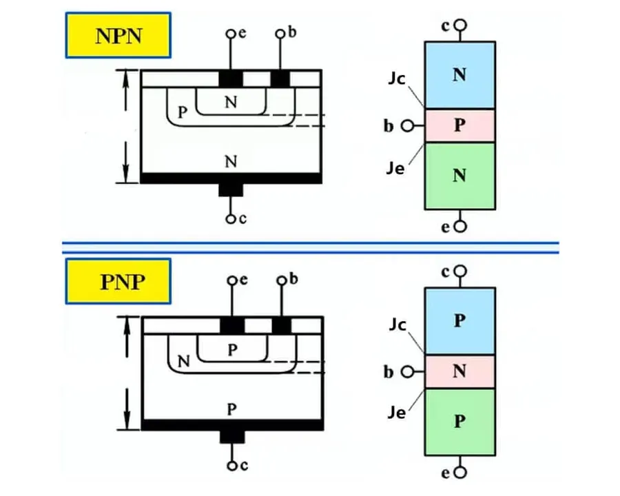
A Bipolar Junction Transistor (BJT) is a fundamental three-terminal semiconductor device that controls electrical current flow. Distinct from unipolar transistors like MOSFETs, BJTs are current-controlled devices, relying on both electrons and holes as charge carriers. This dual-carrier mechanism enables BJTs to perform crucial functions in electronic circuits, including amplification and switching.
The BJT's operation is characterized by the interaction of three differently doped semiconductor regions forming two junctions. These regions are named the emitter, base, and collector, each with specific roles in the transistor's operation. The base acts as the control input, modulating current flow between the collector and emitter. A small current applied to the base can enable or restrict the passage of a significantly larger current between the other two terminals, providing the functionality of both a switch and an amplifier.
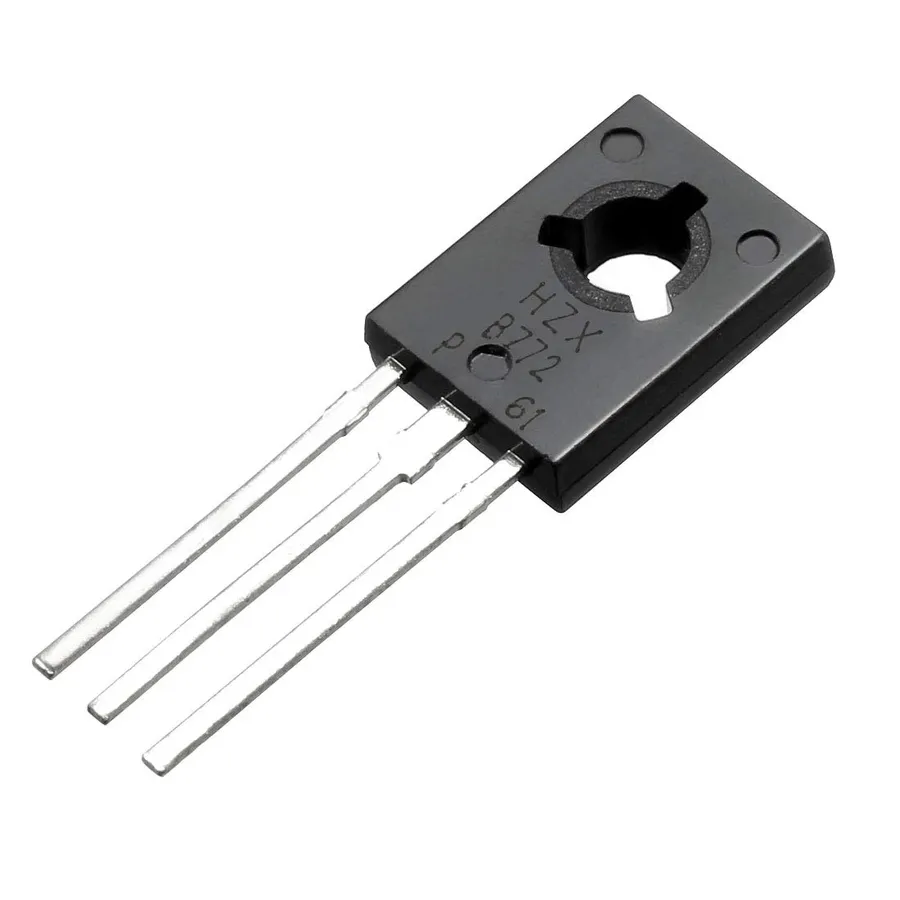
Bipolar Junction Transistors (BJTs) are three-terminal semiconductor devices pivotal in modern electronics, distinguished by their unique construction and the crucial roles of each terminal. Understanding the structure of BJTs, particularly the arrangement of their terminals and the embedded PN junctions, is essential for comprehending their operation and application.
A BJT's construction consists of three distinct layers of doped semiconductor material, forming two PN junctions. These layers, which are either doped with an excess of electrons (n-type) or holes (p-type), are arranged to create either an NPN or PNP configuration. Each configuration dictates the direction of current flow within the transistor.
| Terminal | Description | Role | NPN Configuration | PNP Configuration |
|---|---|---|---|---|
| Base (B) | The middle layer between the emitter and collector. | Controls current flow between collector and emitter. | P-type material | N-type material |
| Collector (C) | One of the outer layers, often with a larger area than the base. | Collects the current carriers. | N-type material | P-type material |
| Emitter (E) | The other outer layer, which supplies charge carriers. | Emits current carriers. | N-type material | P-type material |
The NPN transistor features a p-type base sandwiched between two n-type layers (emitter and collector), while the PNP transistor has an n-type base between two p-type layers (emitter and collector). The distinction in doping profiles between these two types leads to a reversal in the direction of current flow through the transistor.
In practical use, proper biasing is necessary to ensure the transistor functions correctly. The base-emitter junction is typically forward biased, while the base-collector junction is reverse biased. This biasing enables the small base current to modulate the larger current flow between the collector and the emitter, providing the amplifying or switching effect. A key to BJT function is that the base current controls the larger current between the collector and the emitter.
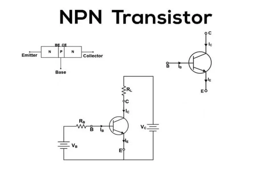
Bipolar Junction Transistors (BJTs) function as current-controlled devices, meaning a small current at the base terminal regulates a larger current flow between the collector and emitter terminals. This fundamental principle of operation underlies the BJT's utility in amplification and switching applications.
The core of a BJT's operation hinges on the interaction of charge carriers within its semiconductor structure. Unlike field-effect transistors (FETs) which utilize an electric field, BJTs rely on the injection and collection of both electrons and holes—hence the term 'bipolar'. The behavior of these charge carriers within the transistor gives rise to its distinct operating regions: active, saturation, and cutoff.
In the active region, the transistor behaves as an amplifier. A small change in base current results in a proportionally larger change in the collector current. This linear relationship makes BJTs ideal for signal amplification. Saturation occurs when the transistor is fully 'on', effectively acting as a closed switch, maximizing current flow from collector to emitter. Conversely, in the cutoff region, the transistor is 'off' with minimal current flowing, acting as an open switch.
Specifically, for an NPN transistor, a small base current injects electrons into the base region, enabling a much larger current flow from the collector to the emitter. For a PNP transistor, current flow direction are reversed, holes are the primary carrier, requiring base current to extract holes from the base, allowing current from emitter to collector. This ability to modulate current with small base current makes bipolar transistors versatile for different circuit needs.
| Operating Region | Base-Emitter Junction Bias | Collector-Base Junction Bias | Transistor Behavior |
|---|---|---|---|
| Active | Forward Biased | Reverse Biased | Amplification; Linear Relationship Between Input and Output Currents |
| Saturation | Forward Biased | Forward Biased | Switch fully 'ON'; Maximum current flow from collector to emitter (or emitter to collector in PNP) |
| Cutoff | Reverse Biased | Reverse Biased | Switch 'OFF'; Minimal current flow |
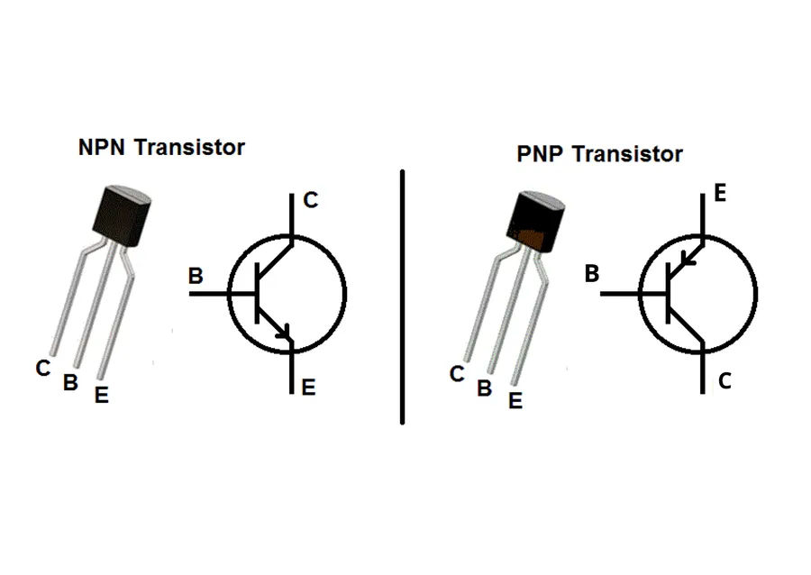
Bipolar junction transistors (BJTs) fundamentally come in two flavors: NPN and PNP. These designations refer to the arrangement of the semiconductor materials—N-type (doped with impurities that contribute free electrons) and P-type (doped with impurities that contribute 'holes,' or electron deficiencies)—within the transistor's structure. The choice between NPN and PNP transistors significantly impacts circuit design, dictating current flow direction and biasing requirements.
| Feature | NPN Transistor | PNP Transistor |
|---|---|---|
| Structure | N-type - P-type - N-type | P-type - N-type - P-type |
| Current Flow (Conventional) | Collector to Emitter (positive charge carriers) | Emitter to Collector (positive charge carriers) |
| Majority Charge Carriers | Electrons | Holes |
| Base Current Direction | Into Base | Out of Base |
| Polarity for Active Region | V_CE > 0, V_BE > 0 | V_CE < 0, V_EB > 0 |
| Use Cases | Common in digital circuits, switching applications, and low-side drivers | Common in high-side switching, analog circuits, and power applications |
The fundamental differences in structure dictate the bias and current flow characteristics. An NPN transistor has an N-type collector and emitter with a P-type base, while a PNP transistor is composed of a P-type collector and emitter with an N-type base. These differences are critical for circuit design.
Below is a simplified circuit diagram representation of both NPN and PNP transistors. Note the direction of the arrow on the emitter, indicating the conventional direction of current flow. In the NPN transistor, the current flows from the collector to the emitter, whereas in the PNP transistor, the current flows from the emitter to the collector. The base current controls the current flow between the collector and the emitter, regardless of the transistor type.
Understanding the key parameters of bipolar transistors is essential for effective circuit design and application. These parameters dictate how a transistor will perform in a circuit, influencing amplification, switching speeds, and power handling capabilities. Crucially, these parameters are not constant; they can vary with temperature, operating conditions, and manufacturing variations, hence understanding their implications is paramount.
| Parameter | Symbol | Description | Impact on Circuit Design |
|---|---|---|---|
| Current Gain | β (Beta) or hFE | Ratio of collector current to base current in common-emitter configuration. Indicates the transistor's ability to amplify current. | Determines amplification factor; affects the gain of amplifier circuits. A higher β allows a smaller base current to control a larger collector current. |
| Collector-Emitter Saturation Voltage | VCE(sat) | Voltage drop between collector and emitter when the transistor is in saturation region (fully ON). | Indicates minimum voltage drop when the transistor is used as a switch. A lower VCE(sat) means lower power loss. |
| Breakdown Voltage | VCEO, VCBO, VEBO | Maximum reverse voltage that can be applied across specified terminals before the transistor breaks down. | Determines safe voltage operating limits. Exceeding breakdown can damage the transistor. |
| Base-Emitter Voltage | VBE | Voltage across base and emitter junction. Necessary for forward biasing the transistor. | Typically around 0.7V for silicon based transistors. Influences the biasing network design. |
| Transition Frequency | fT | Frequency at which the current gain drops to unity. Defines the maximum operating frequency of the transistor. | Defines the bandwidth of amplifier and switching speeds. For high-frequency applications, a higher fT is desirable. |
| Output Conductance | hoe | Change in collector current with respect to change in collector-emitter voltage for a constant base current. | Affects the output impedance. An ideal BJT would have zero output conductance. |
Bipolar transistors, owing to their versatile current-controlling capabilities, are foundational components in numerous electronic applications. Their ability to function as amplifiers and switches makes them indispensable across diverse electronic systems.
| Application | Function | Real-World Examples |
|---|---|---|
| Audio Amplifiers | Amplify weak audio signals to drive speakers. | Stereo systems, headphones, public address systems |
| Switching Circuits | Control on/off states of electronic devices. | Digital logic gates, motor control, power converters |
| Power Supplies | Regulate and convert electrical power. | Linear power supplies, SMPS(switched mode power supplies), DC-DC converters |
| Signal Generators | Produce periodic waveforms for various applications. | Radio transmitters, clock circuits, testing equipment |
| Motor Controls | Control speed and direction of electric motors. | Industrial automation, robotics, electric vehicles |
In essence, the bipolar transistor's core characteristics make it a fundamental building block across diverse electronic systems where amplification, switching, and precise control are essential. They are integral to both analog and digital circuits and ensure precise power control in electrical applications.
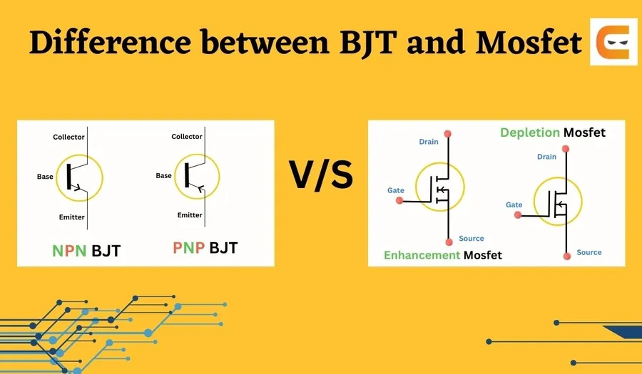
Bipolar Junction Transistors (BJTs) and Metal-Oxide-Semiconductor Field-Effect Transistors (MOSFETs) are the two foundational pillars of modern transistor technology, yet they differ substantially in their operation, characteristics, and ideal applications. Understanding these differences is crucial for effective circuit design and optimization. This section provides a detailed comparison, elucidating the strengths and weaknesses of each technology.
| Feature | Bipolar Junction Transistor (BJT) | Metal-Oxide-Semiconductor Field-Effect Transistor (MOSFET) |
|---|---|---|
| Operation Principle | Current-controlled device; current at the base controls a larger current between the collector and emitter. | Voltage-controlled device; voltage at the gate controls the current between the drain and source. |
| Charge Carriers | Both electrons and holes contribute to current flow (bipolar). | Current flow primarily due to either electrons (n-channel) or holes (p-channel) (unipolar). |
| Input Impedance | Lower input impedance, which means it draws some current from the driving circuit. | Very high input impedance, meaning it draws negligible current from the driving circuit. |
| Gain | Typically higher current gain. | Higher voltage gain is achievable |
| Switching Speed | Generally slower switching speeds due to minority carrier storage effects. | Faster switching speeds, making them suitable for high-frequency applications. |
| Temperature Sensitivity | More susceptible to temperature variations, which can affect current gain. | Less temperature-sensitive and more stable over a wide temperature range. |
| Circuit Complexity | Typically require more complex biasing circuits, often necessitating resistors and capacitors. | Simpler biasing circuits with fewer external components are often needed. |
| Power Handling | Good for high current, high power applications. | Better suited for low power applications, but high power devices are available |
| Applications | Used in analog circuits, amplifiers, power electronics, and discrete designs. | Dominant in digital circuits, microprocessors, memory, and integrated circuits. |
| Cost | Generally lower cost due to relatively simpler manufacturing processes. | Higher manufacturing costs due to the complex gate oxide layer |
This section addresses common questions regarding bipolar junction transistors (BJTs), providing concise and authoritative answers to clarify their usage, characteristics, and relevance in modern electronics.
The field of bipolar transistor technology, while mature, continues to evolve through ongoing research and development efforts. These innovations focus on enhancing performance, efficiency, and exploring novel applications. The relentless pursuit of miniaturization, improved power handling, and higher frequency operation drives the exploration of new materials and fabrication techniques, potentially leading to the development of next-generation bipolar transistors.
Bipolar transistors, often operating behind the scenes, are indeed the unsung heroes of electronics. Their ability to amplify and switch electrical signals makes them essential components in a vast range of devices. While other technologies emerge, bipolar transistors continue to be integral, finding new applications and undergoing continuous advancement. Understanding these fundamental devices is essential for anyone delving into the world of electronics and technology, as their influence will continue to shape our digital future.

