AnyPCBA PCB and PCBA case studies


Our client, a developer of high-performance networking infrastructure, needed a 10G high-speed backplane for their next-generation system. The backplane required thousands of 10G differential pairs across 28 layers, presenting extreme signal integrity challenges that demanded a systematic engineering approach.
Key Technical Challenges:
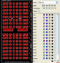
High Layer Count: 28-layer board requiring precise layer stackup design and manufacturing control
High-Speed Signals: Thousands of differential pairs carrying 10G signals
Signal Integrity Critical: Every 10G differential pair required careful impedance control, loss management, and crosstalk mitigation
Multiple Stakeholder Coordination: Required tight collaboration among customer, connector suppliers, and PCB manufacturer
AnyPCBA provided a complete design and signal integrity solution, integrating pre-simulation, constraint-driven design, and post-simulation verification.
Our engineering approach included:
Cross-Functional Collaboration: Worked closely with the customer, connector suppliers, and PCB fabricators from the earliest design stages — ensuring material selection, connector placement, and manufacturing capabilities were aligned before layout began
Pre-Simulation: Performed early-stage signal integrity simulations to evaluate design feasibility, establish routing strategies, and define impedance and loss targets
Constraint-Driven PCB Design: Translated simulation results into specific routing rules — trace width, spacing, length matching, and via design — to ensure signal integrity requirements were met throughout the design process
Post-Simulation Verification: Conducted comprehensive post-layout simulations to verify that all 10G differential pairs met the required signal quality specifications
Design for Manufacturing: Collaborated with the PCB fabricator to optimize the 28-layer stackup and ensure manufacturability of the high-density backplane
| Parameter | Specification |
|---|---|
| Product Type | 10G High-Speed Backplane |
| Layer Count | 28 layers |
| Signal Rate | 10G per differential pair |
| Signal Density | Thousands of high-speed differential pairs |
| Key Challenges | Signal integrity, impedance control, loss management |
| Engineering Workflow | Pre-simulation → Constraint-driven design → Post-simulation |
| Collaboration | Customer, connector suppliers, PCB fabricator |
First-Pass Success: First prototype was debugged successfully with no major signal integrity issues
Signal Quality Verified: Post-simulation confirmed all 10G signals met the required specifications
Reduced Risk: Cross-functional collaboration eliminated material and connector compatibility risks
Cost Savings: First-pass success eliminated costly re-spins and accelerated the customer's validation process
Proven Methodology: Demonstrated the value of systematic SI engineering for high-speed designs
This case demonstrates AnyPCBA's capability to handle the most demanding high-speed backplane projects through systematic engineering and cross-functional collaboration:
✅ High-layer-count expertise (28 layers)
✅ 10G+ high-speed signal design
✅ Complete SI workflow (pre-simulation → constraint-driven design → post-simulation)
✅ Multi-stakeholder coordination (customer, connector suppliers, PCB fabricator)
✅ First-pass success (reduced time-to-market)
Ready to discuss your 10G or high-speed backplane project? Contact us to learn how AnyPCBA can support your design and manufacturing needs.