AnyPCBA PCB and PCBA case studies


Our client, a telecommunications equipment manufacturer, needed a high-complexity communication board for their next-generation networking infrastructure. The board required extremely high component density, large form factor, and mixed assembly technologies to meet the performance demands of modern communication systems.
Key Manufacturing Challenges:
High Component Density: 1978 solder joints and 213 unique component types on a large 282 x 201mm board
Ultra-Fine Pitch Placement: 01005 passive components and 0.3mm pitch BGA packages
Mixed Assembly Technology: Combination of surface-mount (SMT) and through-hole components requiring dual reflow + selective wave soldering
Large Board Size: 282 x 201mm with stringent flatness requirements for reliable assembly
Communication-Grade Reliability: Must meet high signal integrity and long-term reliability standards
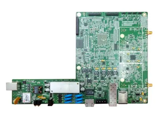
AnyPCBA provided comprehensive manufacturing services for this communication board, from process engineering to full-scale production.
Our manufacturing approach included:
Precision SMT Assembly: Advanced placement equipment capable of 01005 components and 0.3mm pitch BGA with high accuracy
Specialized Soldering Processes: Double reflow for SMT components followed by selective wave soldering for through-hole parts, with custom fixture design to protect assembled areas
Large Board Process Control: Optimized handling and reflow profiles for 282 x 201mm boards to ensure consistent solder joint quality and prevent warpage
Process Optimization: Developed specific solder paste printing profiles and reflow temperature curves to accommodate diverse component requirements
Rigorous Quality Control: Implemented AOI, X-ray inspection (for BGA and hidden joints), and in-circuit testing (ICT)
Material Management: Systematic handling of 213 component types to prevent mix-ups and ensure traceability
Reliability Assurance: Signal integrity testing and functional validation to ensure performance in communication systems
| Parameter | Specification |
|---|---|
| Total Solder Joints | 1,978 |
| Component Types | 213 |
| Board Size | 282 x 201 mm |
| Assembly Process | Double reflow + selective wave soldering |
| Minimum Component Size | 01005 |
| Minimum BGA Pitch | 0.3mm |
Successful Production: Delivered high-quality communication boards meeting all specifications
Process Capability: Demonstrated expertise in advanced assembly technologies (01005, 0.3mm BGA, mixed process)
Large Board Expertise: Proven ability to handle large-format PCBs with consistent quality
Quality Assurance: Comprehensive testing ensured field reliability for communication applications
Supply Chain Management: Efficient handling of 213 component types without delays or errors
Manufacturing Excellence: Demonstrated capability to handle complex, high-density, mixed-technology PCBA projects
This case demonstrates AnyPCBA's capability to handle demanding PCBA manufacturing challenges for telecom and networking applications:
✅ Large-format board processing (up to 282 x 201mm and beyond)
✅ Fine-pitch placement (01005, 0.3mm BGA)
✅ Mixed assembly processes (SMT + through-hole)
✅ High component variety (213+ types per board)
✅ Communication-grade quality systems
Ready to discuss your communication board or high-complexity PCBA project? Contact us to learn how AnyPCBA can support your manufacturing needs.