AnyPCBA PCB and PCBA case studies


Our client, a developer of compact, high-performance electronic devices, needed a high-density interconnect (HDI) PCB that could accommodate complex routing in a limited board space. The design required advanced HDI structures, fine lines, and laser-drilled microvias to achieve the required signal routing density and performance.
Key Manufacturing Challenges:
Complex HDI Structure: 10-layer board with 3+4+3 HDI build-up architecture
Ultra-Fine Lines: 2.4/2.4mil (approx. 0.061mm) line width and spacing
Microvia Drilling: 0.1mm laser-drilled microvias for high-density interconnections
Precise Impedance Control: Tight impedance tolerance requirements for signal integrity
High Reliability: ENIG surface finish for excellent solderability and oxidation resistance
Layer-to-Layer Registration: Tight alignment requirements for HDI sequential lamination
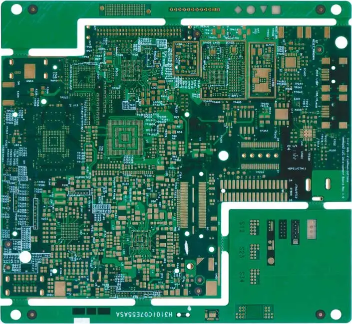
AnyPCBA provided comprehensive PCB fabrication services for this HDI board, from engineering review to final electrical testing.
Our manufacturing approach included:
HDI Process Engineering: Designed and optimized the 3+4+3 sequential lamination process for the 10-layer structure
Fine Line Etching: Advanced etching process control to achieve 2.4/2.4mil line width/spacing with high yield
Laser Drilling: Precision CO2 laser drilling for 0.1mm microvias with controlled via wall quality
Impedance Control: Carefully designed stack-up and controlled etching parameters to meet tight impedance specifications
Sequential Lamination: Precise layer-to-layer registration control for the complex HDI build-up
Surface Finish: ENIG (Electroless Nickel Immersion Gold) for flat, oxidation-resistant surface
Rigorous Testing: Comprehensive electrical testing, including flying probe and impedance testing
| Parameter | Specification |
|---|---|
| Layer Count | 10 layers |
| HDI Structure | 3+4+3 (sequential lamination) |
| Board Thickness | 1.2mm |
| Minimum Line Width/Space | 2.4/2.4mil (approx. 0.061mm) |
| Minimum Laser Hole | 0.1mm |
| Minimum PP Thickness | 2.2mil |
| Surface Finish | ENIG (Electroless Nickel Immersion Gold) |
| Application | High-density electronic devices |
Successful Fabrication: Delivered high-quality 10-layer 3+4+3 HDI PCBs meeting all specifications
Fine Line Capability: Demonstrated ability to fabricate 2.4/2.4mil line width/spacing with high yield
HDI Expertise: Proven capability in complex HDI structures and sequential lamination processes
Precision Manufacturing: Achieved 0.1mm microvia drilling with excellent quality
Signal Integrity: Tight impedance control ensured reliable high-speed signal transmission
Reliable Finish: ENIG surface finish provided excellent solderability and long-term reliability
This case demonstrates AnyPCBA's capability to handle demanding PCB fabrication challenges for high-density, compact electronic designs:
✅ Complex HDI structures (10-layer, 3+4+3 sequential lamination)
✅ Ultra-fine lines (2.4/2.4mil line width/spacing)
✅ Precision laser drilling (0.1mm microvias)
✅ Tight impedance control (for signal integrity)
✅ High-reliability surface finish (ENIG)
Ready to discuss your HDI PCB or high-density design project? Contact us to learn how AnyPCBA can support your PCB fabrication needs.