
AnyPCBA PCB and PCBA case studies


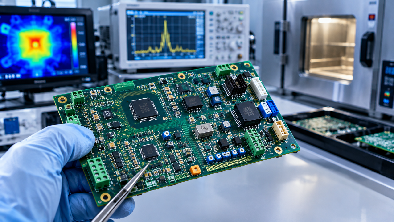
Introduction: A real-world case study of an industrial temperature control PCB: 4-channel PT100 acquisition + 2-channel TEC drive, targeting ±0.1°C stability. The early 4-layer version showed periodic PT100 drift under full TEC load. Root cause analysis revealed that power noise, thermal paths, and stack-up design—not ADC resolution—were the real limits.
Description: Based on AnyPCBA's small-to-medium volume PCB and PCBA manufacturing experience, this case study explains how power path design, thermal-sensitive component placement, and 8-layer stack-up optimization solved a temperature control accuracy problem—and how DFM review catches these risks at the design stage.
A customer needed a domestic industrial-grade temperature control mainboard for a constant-temperature bath controller:
Operating temperature: -40°C to +85°C
Channels: 4-channel PT100 acquisition + 2-channel TEC drive
Target accuracy: ±0.1°C
But in the early 4-layer version, after 5 minutes of full TEC load, the PT100 reading began drifting with a 1.2 Hz rhythmic pattern—not random jumps, but a breathing-like oscillation.
This was not a failed ADC, nor a PID tuning issue. The PCB was "speaking"—electrical, thermal, and field effects are never three separate things, but three faces of one system.
The customer did three things:
Thermal imaging: LDO area temperature rose 15°C; REF3025 pad reached 68°C, exceeding its temperature drift specification.
Spectrum capture: A 1.23 MHz peak was captured at the INA128 input—the second harmonic of the Buck switching frequency (1.2 MHz).
Thermal-electrical co-simulation: ANSYS Icepak + HFSS confirmed the noise path: LDO output → REF3025 → ADS124S08 REF pin.
Root cause: The LDO is not a filter—it is the last door, not the whole path. If a pile of switching noise "garbage" is stacked in front of the door, even the best door cannot stop the smell from seeping in.
The power chain is a "three-stage purification channel":
| Stage | Target Frequency | Key Design |
|---|---|---|
| Input purification | 10 kHz–1 MHz | π-type LC filter: 22 μF + 1 μH ferrite bead + 10 μF. Ferrite bead must meet 100 Ω @ 100 MHz, DCR < 0.15 Ω |
| Mid-stage isolation | 1–100 MHz | Buck does not directly feed LDO. First through 47 μF low-ESR tantalum + 100 Ω @ 100 MHz ferrite bead, then LT3045 (PSRR 79 dB @ 1 MHz) |
| End-stage anchoring | >100 MHz | LDO output to ADC VDD: 0.1 μF + 10 μF in parallel, 0.1 μF placed tight against VDD pad, trace length ≤0.5 mm |
The most critical detail is in the "ground" treatment: Instead of the textbook "split ground + 0 Ω bridge," the AGND and DGND connection point was precisely placed at the GND pad of the LT3045 input capacitor—the most stable ground potential point in the entire analog domain. Bridging at this point anchors the analog ground "zero potential" at the noise valley, not the noise peak.
Power-up sequencing is another hidden pitfall: The STM32H7 VDDA internal LDO needs about 300 μs to start, while the external LT3045 needs 100 μs from enable to stable output. If the MCU pulls LDO_EN high immediately on power-up, REF3025 gets "shaken" and the first sample value collapses. A 10 ms delay in firmware closes this loophole.
PCB copper is an efficient thermal conductor (λ ≈ 390 W/m·K), 1300 times faster than FR-4. A 2 mm wide copper pour can transfer heat faster than a 1 cm thick air layer. So "isolating heat sources" is not about distance—it is about "cutting the copper thermal path."
The board is divided into three physical thermal zones:
Heat source zone (bottom right): TEC drive MOSFET, Buck inductor, heatsink. A 2 mm wide thermal slot is cut in the bottom layer to block vertical heat conduction. No vias are allowed under power device pads to connect to inner ground layers.
Buffer zone (middle): MCU, Flash, RS-485 isolation chip. Copper pour uses a 50% grid pattern, reducing effective thermal conductivity to ≈15 W/m·K—maintaining signal return while weakening lateral heat spread.
Sensitive zone (top left): PT100 terminals, REF3025, ADS124S08, crystal. No large copper pours allowed—only necessary trace-width "ground lines" are kept. For temperature-sensitive devices, a "ground plane" is a thermal blanket, not a shield.
The 8-layer stack-up is arranged as follows:
| Layer | Function | Description |
|---|---|---|
| L1 | Signal | Top: high-speed digital, PGND copper |
| L2 | GND | Digital return main path, tightly coupled with L1 |
| L3 | Signal | Analog signal layer: PT100, ADC REF, op-amp inputs |
| L4 | Power | Split power plane: VDDA / VDDD / VTEC, 20 mil gap |
| L5 | GND | Analog return main path, tightly coupled with L3/L4 |
| L6 | Signal | Digital signal layer: MCU peripherals, RS-485 |
| L7 | GND | TEC drive return, single-point connection to L5 |
| L8 | Signal | Bottom: thermal slots, PGND copper, mounting holes |
The elegance: L2 and L5 dual ground layers sandwich L3 (analog signal) like a three-layer sandwich. Signal return current is naturally "pulled" to the nearest ground layer, forming an extremely short loop. The L4 power plane is fully shielded by two ground layers—switching noise cannot penetrate the "ground-power-ground" structure.
Thermal design: L2/L5 ground layers are thickened from 1 oz to 2 oz, while L3/L6 signal layers stay at 1 oz. This "thick ground, thin signal" structure reduces overall thermal resistance by 37%, and the TEC drive area surface temperature rise drops from 52°C to 41°C.
Dielectric material: Core layers use RO4350B (εr=3.66, Df=0.0037). It costs 30% more, but high-frequency loss is 15% lower than FR-4, and its CTE matches copper better—less warpage under wide temperature cycles.
After the system redesign, the customer's measured results:
PT100 reading fluctuation converged to ±0.05°C
ADS124S08 ENOB improved from 19.2 bit to 21.7 bit
RS-485 bit error rate remained stable at 10⁻⁹ under 4 kV EFT strike
The ceiling of temperature control accuracy is often not determined by ADC resolution, but by the few millimeters of copper routing, the 0.3 mm via diameter, and the 10 ms power-up delay on the PCB.
This case is one of the typical engineering experiences AnyPCBA has accumulated in small-to-medium volume PCBA manufacturing. Our role is not just to build to the drawing—we step in at the DFM review stage to help customers identify these "invisible physical path" risks.
In this project, AnyPCBA was involved in:
Stack-up structure review: confirming the lamination process window for 2 oz thick copper ground layers, and layer-to-layer alignment requirements for RO4350B and FR-4 hybrid lamination
Thermal management process support: evaluating depth-controlled milling precision for thermal slots, and manufacturability of "no vias" under power device pads
Via process confirmation: drilling precision and hole wall quality for 0.3 mm via arrays
Power-up sequencing verification support: working with the customer to capture timing waveforms and confirm batch consistency of the 10 ms delay window
Our manufacturing capabilities cover 2–64 layers, including HDI, rigid-flex, and high-frequency hybrid. We hold ISO 13485 (medical) and IATF 16949 (automotive) certifications, with extensive experience in temperature control, medical, and industrial high-precision applications.
If you're designing a high-precision temperature control PCB, or facing similar accuracy bottlenecks, contact us through our website. Our engineers can help you anticipate these "physical-path-determined" performance risks at the design stage.


