AnyPCBA PCB and PCBA case studies


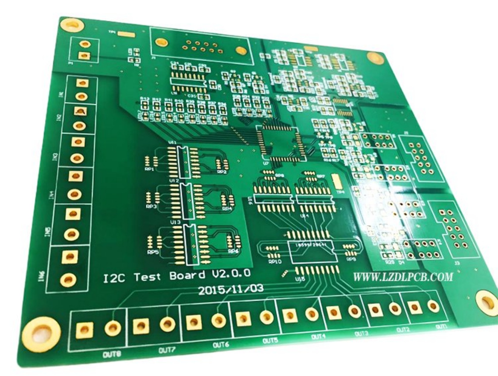
High-speed digital circuit boards are the core carriers of embedded systems, communication equipment, and computing boards. These boards typically use an FPGA or high-performance processor as the core, with external DDR memory, running at speeds ranging from hundreds of Mbps to tens of Gbps. As signal rates continue to climb, PCB design complexity has shifted from "connecting correctly" to "maintaining signal integrity."
AnyPCBA has extensive experience in the design and manufacturing of high-speed digital circuit boards. This case study uses a typical FPGA/processor + DDR memory architecture to systematically outline the key design and manufacturing considerations for stackup design, impedance control, power integrity, decoupling networks, and differential pair routing.
High-speed digital board design faces multiple challenges:
| Challenge | Requirements | Design Difficulty |
|---|---|---|
| Signal Integrity | Eye diagram quality, timing margin, data integrity | Impedance discontinuity, reflection, crosstalk, ISI |
| Power Integrity | Low-impedance PDN, low ripple | Voltage drop on high-current paths, decoupling placement, plane resonance |
| Timing Matching | DDR data/address/control group length matching | Errors controlled at mil or ps levels |
| Return Path | Low-inductance return for high-speed signals | Reference plane transitions, stitching capacitor design |
| EMI Control | Meeting radiated emission standards | Clock signal treatment, differential routing, ground shielding |
High-speed digital boards must use 4 or more layers. Typical stackups include:
Signal – GND – VCC – Signal: Suitable for medium-complexity designs
Signal – GND – Signal – GND/PWR: Suitable for high-density routing
Signal – GND – Signal – VCC – GND – Signal: Suitable for high-speed interface-intensive scenarios
Core principle: Provide a complete, low-impedance reference plane for every high-speed signal layer. Reference plane integrity directly determines return path quality — any split or slot forces the return current to detour, increasing loop area and EMI radiation.
Beneath the core processor/FPGA and DDR memory areas, large, unsplit power and ground planes must be provided.
Key design points:
High-speed signal return paths primarily flow through the ground plane — ground plane integrity is critical
For multi-power-domain designs (core voltage, DDR voltage, I/O voltage), multiple power layers are often needed; each power layer should remain as complete as possible
Power and ground planes should be tightly coupled (spacing ≤ 4 mil) to form effective planar capacitance and reduce high-frequency noise
DDR Memory Interface:
| Signal Group | Matching Requirement | Tolerance |
|---|---|---|
| Intra-pair | DQS+/DQS- length matching | ≤ 5 mil |
| DQ group | Data line length matching | ≤ 10 mil |
| Address/Control | Group length matching | ≤ 20 mil |
| Clock vs. Data | Timing matching | ps level |
High-Speed Signal Impedance Control:
Single-ended signals: 50Ω
Differential signals: 100Ω
Impedance tolerance controlled within ±5% through stackup calculation and controlled-depth fabrication
Layer Transitions and Stitching Capacitors:
Avoid layer transitions for critical high-speed traces. If a transition is unavoidable, add a stitching capacitor near the via to connect the two reference planes (typically GND), providing a low-inductance return path.
Dense decoupling capacitor arrays should be placed around the processor/FPGA, covering different frequency ranges:
| Capacitor Type | Value | Frequency Range | Placement |
|---|---|---|---|
| Ceramic | 100 nF | High frequency | Closest to power pins |
| MLCC | 10 μF | Mid frequency | Near power pins |
| Tantalum/Polymer | 100 μF+ | Low frequency | Can be farther, provides bulk energy |
Core principle: Place capacitors as close as possible to power pins, prioritizing the highest-frequency capacitors.
High-speed serial signals (PCIe, USB, SATA, Ethernet PHY) must follow strict differential pair routing rules:
Equal length: Intra-pair length matching
Equal spacing: Constant spacing maintained
Parallel routing: Avoid unnecessary bends
Spacing control: Keep sufficient spacing (≥ 3× trace width) from other traces
Clock lines are the most critical noise sources and require special treatment:
Priority routing: Route clock lines first during layout
Shortest path: Minimize trace length
Keep away from sensitive circuits: Avoid proximity to I/O ports or sensitive analog circuits
Ground shielding: Use copper pour above/below or on both sides to form a shield when necessary
Buck converter modules supplying high-current loads (such as processors) should be placed as close as possible to the load:
Shorten high-current paths, reduce voltage drop and inductance
Optimize thermal paths, reduce thermal resistance
Reduce power noise coupling
| Outcome Dimension | Value Delivered |
|---|---|
| Signal Integrity | Eye diagram opening meets specifications, data integrity guaranteed |
| Timing Margin | DDR interface timing margins meet strict requirements |
| Power Integrity | Power noise controlled within target range, decoupling network effective |
| EMI Performance | Meets radiated emission standards, reduces electromagnetic interference |
| System Stability | High-speed signal transmission stable, reliable system operation |
Embedded system main control boards
Communication equipment processing boards
Computing accelerator cards and data acquisition boards
FPGA development boards and prototype verification platforms
Industrial control and edge computing devices
This project demonstrates AnyPCBA's core capabilities in high-speed digital PCB design and manufacturing:
✅ High-speed signal integrity — impedance control, length matching, return path optimization
✅ Power integrity — complete plane design, decoupling network optimization, low-impedance PDN
✅ Multilayer manufacturing — 4-64 layer stackups, HDI, high-frequency hybrid processes
✅ DFM design review — identifying signal integrity and manufacturability issues during design phase
✅ Prototype to production — supporting small-batch to medium-volume production
Need High-Speed Digital PCB Design and Manufacturing Support?
AnyPCBA has extensive experience in high-speed digital circuit boards, supporting 2-64 layers with HDI, rigid-flex, and high-frequency hybrid processes. Our engineering team provides DFM/DFA design reviews to help identify potential issues in stackup, impedance, and material selection before fabrication.
Contact us to discuss your project →