
AnyPCBA PCB and PCBA case studies


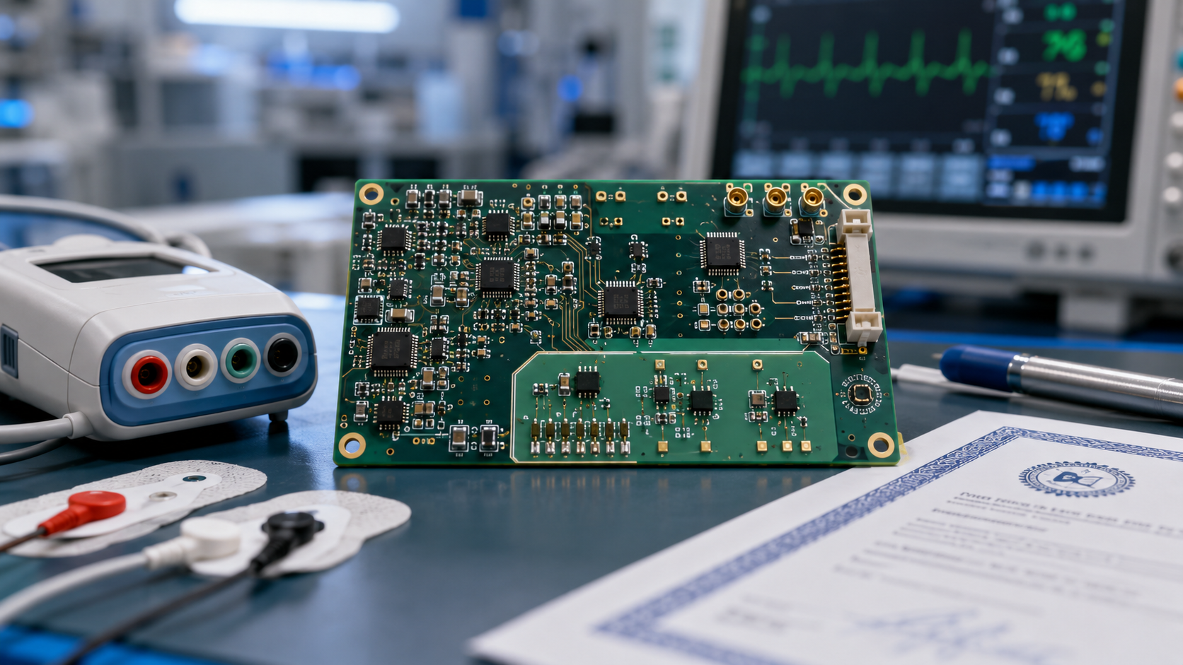
With the rapid growth of telemedicine, home health monitoring, and portable diagnostic devices, the medical electronics industry has placed increasingly stringent demands on PCB signal acquisition accuracy and reliability. Products such as ECG monitors, pulse oximeters, and portable ultrasound devices require high-fidelity analog signal acquisition within compact form factors, while maintaining strict standards for noise suppression, long-term stability, and medical-grade certification.
AnyPCBA holds ISO 13485 medical quality management system certification and has extensive experience in medical electronics PCB design and manufacturing. This case study demonstrates our technical capabilities in high-precision routing, noise suppression, and medical-grade material selection for portable medical device applications.
Portable medical device PCB design faces three core challenges:
| Challenge | Requirements | Design Difficulty |
|---|---|---|
| Signal Acquisition Accuracy | Physiological signal acquisition error ≤1% | Differential pair length mismatch and impedance discontinuity cause signal distortion |
| Noise Suppression | CMRR ≥60dB, noise voltage ≤10μV | Digital noise couples into analog paths through ground loops and spatial coupling |
| Medical-Grade Certification | Compliance with ISO 13485 and IEC 60601-1 | Material selection, process control, and traceability must all meet medical standards |
Analog signals (e.g., ECG, SpO₂) are routed using matched-length differential routing strategies:
Length mismatch controlled to ≤0.5mm
Trace spacing ≥0.3mm, differential impedance at 100Ω±10%
Common Mode Rejection Ratio (CMRR) improved to ≥70dB
Design Guidelines:
Keep differential pairs as close as possible to minimize loop area
Avoid placing vias or other traces between differential pairs
Maintain continuous reference plane integrity under differential traces
Employ a "Analog Ground – Digital Ground – Protective Ground" three-isolation grounding strategy:
Complete isolation between analog, digital, and protective grounds
Single-point connection impedance ≤0.05Ω
Prevents digital noise (from MCU, clocks, etc.) from coupling into analog signal paths
Noise voltage controlled to ≤10μV
Design Guidelines:
Place the single-point connection beneath the ADC or signal conditioning circuitry
Use ferrite beads or 0Ω resistors for isolation
Ensure the shortest, lowest-impedance return path
Low-noise medical-grade laminates are selected to meet signal transmission and long-term reliability requirements:
| Parameter | Specification |
|---|---|
| Dielectric Constant (Dk) | 4.3±0.2 (typical) |
| Dissipation Factor (Df) | ≤0.012@1kHz |
| Analog Signal Transmission Loss | ≤0.1dB/m |
| Moisture Absorption | ≤0.1% (after 120°C/24h baking) |
Selection Principles:
Low Dk variation to ensure consistent impedance
Low Df to minimize attenuation of low-frequency physiological signals
High Tg to meet long-term reliability requirements of medical devices
Design Phase:
Automatic optimization of differential pair length mismatch (≤0.5mm)
Clear zoning of the three-isolation grounding regions
Identification and resolution of ground impedance violations
Manufacturing Phase:
High-precision routing equipment maintaining length mismatch ≤±0.3mm
Heavy copper ground pour (2oz) achieving ground impedance ≤0.04Ω
Strict lamination and drilling process control
Inspection Phase:
Batch sampling testing for signal acquisition error (≤1%) and CMRR (≥60dB)
High-precision oscilloscope and signal generator with 0.05% error detection accuracy
Fully traceable process documentation compliant with ISO 13485
| Outcome Dimension | Value Delivered |
|---|---|
| Signal Acquisition Error | Controlled to ≤1% — exceeding industry average |
| Common Mode Rejection Ratio | ≥60dB — meeting medical device interference immunity requirements |
| Noise Voltage | ≤10μV — ensuring clear acquisition of weak physiological signals |
| Medical-Grade Compliance | Full compliance with ISO 13485 and IEC 60601-1 |
| Manufacturing Yield | Stable process control ensuring high batch-to-batch consistency |
ECG monitor signal acquisition boards
SpO₂ sensor interface boards
Portable ultrasound front-end processing boards
Blood glucose monitor embedded control boards
Remote health terminal data acquisition modules
This project demonstrates AnyPCBA's core capabilities in medical electronics PCB development:
✅ ISO 13485 certified – full medical-grade quality management
✅ High-precision signal integrity – differential routing, impedance control, three-isolation grounding
✅ Medical-grade materials – low-noise laminate selection and process matching
✅ Rigorous DFM review – identifying and resolving potential issues during design phase
✅ Full traceability – from raw materials to finished product testing, meeting medical device regulatory requirements
Need Medical Electronics PCB Design and Manufacturing Support?
AnyPCBA holds ISO 13485 medical quality management system certification and delivers proven solutions for high-precision signal acquisition PCBs in portable medical devices. Our manufacturing capabilities cover 2-64 layers, including HDI, rigid-flex, and high-frequency hybrid processes.
Contact us to discuss your project →


