
AnyPCBA PCB and PCBA case studies


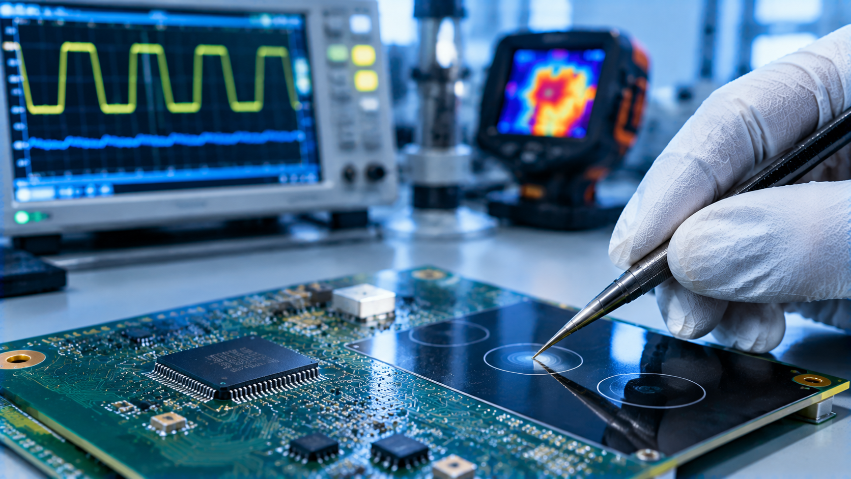
Introduction: A smart home manufacturer faced severe touch panel issues in early 2026: low sensitivity and frequent false triggers caused by electromagnetic interference. This case study reveals how AnyPCBA's DFM engineers identified the root causes—long signal traces, poor isolation from a DC-DC converter, and improper ground pours—and redesigned the layout and manufacturing process to achieve a 99.8% yield rate.
Description: Based on AnyPCBA's manufacturing expertise, this case study explains how we solved touch panel false triggers and low sensitivity in a smart home PCBA by optimizing signal trace length, adding ground isolation, and adjusting ground pours to improve capacitive touch stability.
In early 2026, a smart home manufacturer approached AnyPCBA with a touch panel PCBA.
The panel used the TB2022 touch IC. The customer had strictly followed the "typical application circuit" in the chip datasheet during the design phase. However, after the first small-batch trial production (about 500 units), the factory and the customer both reported the same critical issues:
Low sensitivity: When a user wore slightly thicker gloves, or didn't press firmly against the panel, the touch panel didn't respond at all.
Frequent false triggers: The moment the motor inside the device (like a robot vacuum or smart fan) started up, or when a phone charger was placed nearby, the touch panel would randomly trigger.
The customer had spent two weeks troubleshooting internally and modified the firmware parameters three times, but couldn't completely resolve the issue. This was clearly not a software bug—it was physical interference breaking through the hardware design limits.
To understand why the touch panel failed, we first need to look at how capacitive touch works. The touch IC detects changes in capacitance when a finger approaches the sensor pad.
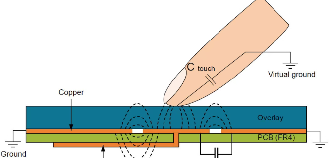
Capacitive touch sensing principle: the finger acts as a virtual ground, changing the capacitance between the sensor pad and the environment.
After receiving the customer's files, AnyPCBA's engineers immediately conducted an in-depth DFM (Design for Manufacturing) review and used a microscope to inspect the physical board. We quickly identified three physical culprits causing the touch failure:
Overly long signal traces without isolation: For routing convenience, the customer had extended the trace from the Sensor Pad to the chip pin to nearly 4cm, and it ran parallel directly through the power trace area, introducing massive parasitic capacitance and crosstalk.
Strong interference sources not mitigated: A high-power DC-DC buck converter on the board was placed extremely close to the Sensor Pad without a shielding isolation band. The high-frequency switching noise from the DC-DC was directly coupled onto the touch signal.
Improper solder mask and copper pour treatment: The customer had used a solid copper pour (GND) directly beneath the Sensor Pad, resulting in excessive initial capacitance and significantly reduced detection sensitivity.
Targeting these issues, AnyPCBA's engineering team worked with the customer to develop a systematic hardware rectification plan:
Shortened signal path: We repositioned the touch chip and its accompanying 0.1μF filter capacitor closer together, forcing the trace length from the Sensor Pad to the chip to be reduced to under 2cm, with a trace width adjusted to 8 mil.
Added shielding isolation: We placed a 2mm-wide GND isolation band between the DC-DC module and the Sensor Pad, with added via stitching to firmly "trap" the interference source.
Adjusted copper pour strategy: We changed the solid copper beneath the Sensor Pad to mesh copper (1–2mm grid spacing), significantly reducing parasitic capacitance and improving sensitivity without compromising interference resistance.
Because the product's enclosure is extremely thin (acrylic thickness only 3mm), the PCB flatness requirements were extremely high. During production, AnyPCBA strictly symmetrized the stack-up and built custom reflow carriers to ensure the PCBA's warpage was below 0.5% at shipment, preventing assembly gaps from causing unstable air dielectric.
During the SMT cleaning stage, ionic contamination on the surface was strictly controlled to ensure insulation performance in the touch area.
After re-prototyping and validation, the reworked PCBA showed excellent stability:
Interference immunity: Under strong interference scenarios such as motor startup or a phone placed nearby, the false trigger rate was 0.
Sensitivity: Even through a 5mm-thick insulating panel, touch response remained extremely smooth.
Production yield: In the subsequent 5,000-unit production order, the factory's ICT/FCT test first-pass yield reached 99.8%, and the customer received no touch-related complaints in the after-sales channel.
Many engineers, when encountering touch issues, look for solutions in firmware algorithms. But the real solution often lies in the physical layout of the PCB. Standardized schematic + refined PCB layout + adaptive panel material is the formula for zero-failure touch control.
In this project, AnyPCBA played not only the role of manufacturer, but also acted as the customer's hardware consultant during the DFM phase, helping them bridge the physical gap from blueprint to mass production.
If you're developing consumer electronics with touch panels, or if your project is experiencing unexplained interference or sensitivity issues during trial production, contact AnyPCBA. Our engineering team excels at finding and eliminating problems based on the underlying logic of manufacturing and physical design.
AnyPCBA focuses on small-to-medium volume PCB and PCBA manufacturing from 5 to 5,000 pieces. For more information, visit our website.


