In today's world of miniaturized electronics, High-Density Interconnect (HDI) PCBs are critical components. From smartphones to medical devices, HDI PCBs enable complex functionality in compact designs. Selecting the right HDI PCB manufacturer is crucial for the success of any project, ensuring quality, reliability, and innovation. This guide dives into the key considerations when choosing an HDI PCB manufacturer, focusing on their capabilities, technologies, and how to make an informed decision for your specific requirements, empowering you to choose the ideal hdi pcb manufacturer.
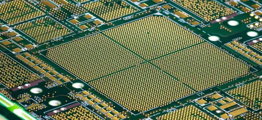
High-Density Interconnect (HDI) PCB technology represents a significant advancement in printed circuit board design, enabling smaller, more complex, and higher-performing electronic devices. At its core, HDI technology focuses on maximizing circuit density by incorporating features like microvias, fine lines, and increased layer counts.
These features directly translate to improved electrical performance by reducing signal path lengths, minimizing impedance mismatches, and enabling higher signal speeds, while decreasing board size.
The defining characteristics of HDI PCBs revolve around these key attributes:
The application of these features enables the production of HDI PCBs that cater to demanding applications in industries such as telecommunications, aerospace, medical and consumer electronics. The ability of an HDI PCB manufacturer to consistently deliver these specific manufacturing capabilities is therefore paramount. The key is to understand these defining characteristics and select a manufacturer that can meet the stringent requirements these characteristics bring.
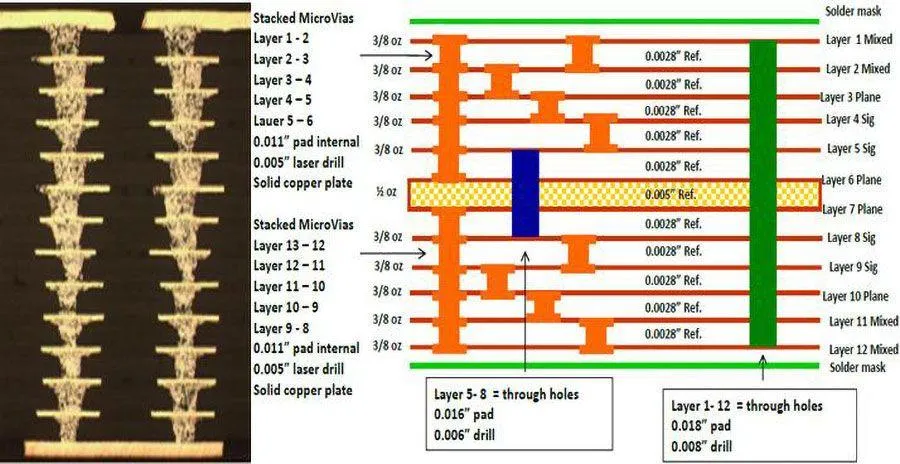
Selecting the right High-Density Interconnect (HDI) PCB manufacturer requires a thorough understanding of their capabilities. HDI PCBs, characterized by their higher wiring density per unit area, demand specialized manufacturing processes. This section outlines the crucial capabilities a manufacturer must possess to produce high-quality HDI PCBs, ensuring optimal performance and reliability.
| Capability | Description | Importance for HDI PCBs |
|---|---|---|
| Laser Drilling | Precision drilling of microvias (small vias) using laser technology. | Essential for creating the dense interconnects required in HDI designs. |
| Sequential Lamination | Adding layers to the PCB in a step-by-step manner. | Enables the creation of complex, multilayer structures typical of HDI PCBs. |
| Fine Line and Spacing Control | Ability to fabricate very thin traces and spaces between them with high accuracy. | Critical for achieving high wiring density and meeting the performance requirements. |
| Advanced Plating Techniques | Specialized processes for uniform copper plating within small vias and fine lines. | Ensures reliable electrical connections and prevents signal loss. |
| Buried and Blind Via Formation | Technology to create vias that connect only some layers, not all. | Allows for complex routing and increased component density, key for HDI applications. |
| Microvia Formation and Filling | Precise microvia creation and filling with conductive material. | Provides reliable connections, enhances electrical performance, and is crucial for HDI design |
| Impedance Control | Maintaining consistent impedance throughout the PCB traces. | Vital for high-speed signal transmission and signal integrity, often a crucial aspect of HDI PCBs. |
| High-Resolution Imaging | Capability to expose and develop very fine patterns on the PCB. | Necessary for creating the intricate patterns found in HDI PCBs. |
| Automated Optical Inspection (AOI) | Automated visual inspection for defects at various stages of production. | Critical for quality control, ensuring that the final product meets specifications and minimizes defects. |
| Electrical Testing | Rigorous testing to ensure electrical connectivity and performance. | Validates the circuit functionality and identifies any potential electrical issues. |
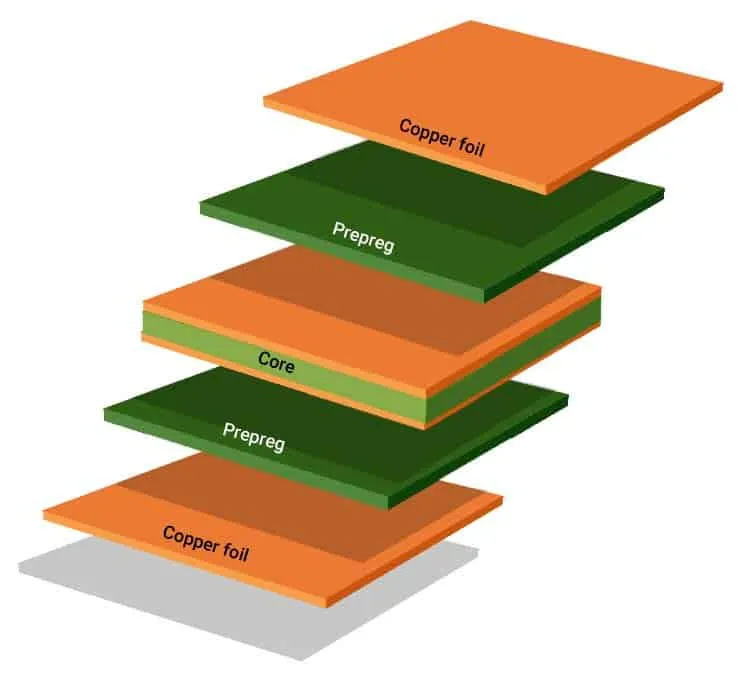
The selection of materials for High-Density Interconnect (HDI) PCBs is paramount, directly impacting the board's performance, reliability, and longevity. Key considerations include the dielectric constant, thermal performance, and mechanical properties of the chosen materials. These factors are crucial for ensuring signal integrity, efficient heat dissipation, and the structural integrity of the HDI PCB.
| Property | Description | Impact on HDI PCB |
|---|---|---|
| Dielectric Constant (Dk) | A measure of a material's ability to store electrical energy. | Lower Dk values generally lead to faster signal transmission and reduced signal loss, crucial for high-frequency applications. |
| Dissipation Factor (Df) | A measure of energy lost as heat in the dielectric material. | Lower Df values minimize signal degradation and heat generation, enhancing signal integrity and efficiency. |
| Thermal Conductivity | A measure of a material's ability to transfer heat. | Higher thermal conductivity allows for efficient heat dissipation, preventing overheating and ensuring long-term reliability. |
| Coefficient of Thermal Expansion (CTE) | A measure of how much a material expands or contracts with temperature changes. | Matching CTE values of materials helps prevent mechanical stress and failures due to thermal cycling. |
| Mechanical Strength | The material's resistance to deformation or fracture. | Ensures the structural integrity of the PCB, withstanding assembly stresses and environmental factors. |
| Moisture Absorption | A measure of how much water a material can absorb. | Lower moisture absorption is preferred for stability and preventing electrical performance degradation over time. |
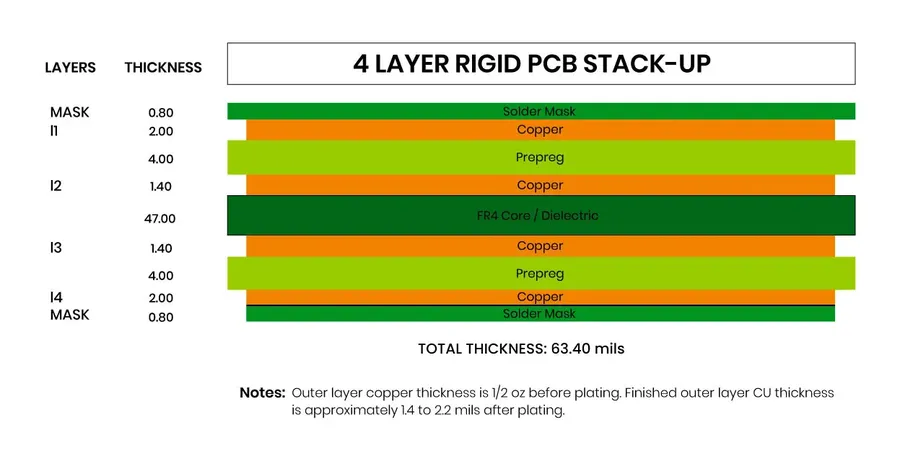
Effective HDI PCB design is crucial for achieving desired performance, and it directly impacts the manufacturer's ability to produce the board according to specifications. This section outlines key design parameters that require careful consideration to ensure both functionality and manufacturability. These parameters include trace width, spacing, via design, and layer stack-up.
| Design Parameter | Description | Impact on Performance | Impact on Manufacturability |
|---|---|---|---|
| Trace Width | The width of conductive paths on the PCB. | Affects signal impedance, current carrying capacity, and signal integrity. | Narrower traces require more precise manufacturing processes; can lead to production challenges if too fine. |
| Trace Spacing | The distance between adjacent conductive paths. | Impacts signal crosstalk, electromagnetic interference (EMI), and insulation. | Smaller spacing requires more accurate etching and placement technologies, potentially increasing manufacturing costs. |
| Via Design | The type, size, and location of vias used to connect different layers. | Affects signal path length, impedance, and thermal management. | Microvias and buried vias require advanced drilling and plating techniques; Improperly placed vias can cause shorts or opens. |
| Layer Stack-Up | The number and sequence of conductive and dielectric layers in a PCB. | Influences impedance control, signal integrity, and power distribution. | Complex stack-ups with multiple layers require precise lamination and alignment, necessitating advanced manufacturing capabilities. |
These design considerations are not isolated; they interact with each other and must be balanced to achieve optimal performance and manufacturability. Close collaboration between the designer and the HDI PCB manufacturer is essential, particularly during the initial stages of design, to ensure that the design can be manufactured efficiently and reliably. Understanding these design constraints and their effects is important to choose the correct hdi pcb manufacturer.
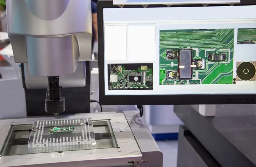
Quality control is paramount in HDI PCB manufacturing due to the intricate nature of these boards, which feature microvias, fine lines, and multiple layers. Rigorous quality control processes are not just about identifying defects; they are essential for ensuring the reliability, performance, and longevity of HDI PCBs, particularly in demanding applications. A reliable HDI PCB manufacturer will implement stringent quality control measures throughout the production process.
This section addresses common queries regarding High-Density Interconnect (HDI) PCBs, providing clear and concise answers to help you better understand this advanced technology and make informed decisions when selecting an HDI PCB manufacturer.
Selecting the right HDI PCB manufacturer requires a thorough comparison across several key factors. This section provides a practical guide to help you differentiate between potential partners based on crucial criteria such as pricing, turnaround time, and technical support, ensuring you make an informed decision tailored to your specific project needs.
| Criteria | Description | Importance in HDI PCB Manufacturing | Questions to Ask |
|---|---|---|---|
| Pricing | The cost per unit or project, including tooling, NRE (Non-Recurring Engineering) charges, and material costs. | Directly impacts project budget and overall cost-effectiveness; HDI PCBs can be more expensive due to their complexity. | What are your pricing tiers based on order volume? Are there any hidden costs? |
| Turnaround Time | The time required from initial design submission to the delivery of finished PCBs, often crucial for project timelines. | Critical for meeting project deadlines; shorter turnaround times often come at a premium, but are essential for time-sensitive projects. | What is your typical lead time for HDI PCBs? Do you offer expedited services? |
| Technical Support | The level of engineering assistance offered, including design feedback, DFM (Design for Manufacturing) analysis, and troubleshooting. | Crucial for resolving design issues, improving manufacturability, and ensuring overall project success. | Do you offer DFM checks? What kind of technical support do you offer throughout the process? |
| Manufacturing Capabilities | Specific technologies and equipment used by the manufacturer to meet HDI PCB requirements, such as laser drilling and sequential lamination. | Indicates the manufacturer's ability to handle the specific requirements of your design. Not all manufacturers have the same HDI capabilities. | Do you have experience in manufacturing this type of HDI PCB? Can you provide technical data sheets related to your capability? |
| Quality Certification | Demonstrates adherence to international quality standards, such as ISO 9001, AS9100, or IPC standards, ensuring consistency and quality control. | Provides assurance that the manufacturer maintains rigorous process controls and quality management systems. | What quality certifications do you hold? Can you show me the results of your internal QC testing? |
| Material Expertise | Understanding and experience of various materials suitable for HDI PCBs, including their electrical and thermal properties. | Essential for selecting materials that match your specific performance requirements, and it speaks to the expertise of the manufacturer. | What kind of HDI PCB materials do you have experience with? What is the benefit of one over another? |
| Communication | How responsive and transparent the manufacturer is regarding project progress, timelines, and any potential problems. | Good communication is vital to a healthy working relationship. Clear communication can prevent costly errors and delays. | How do you keep clients updated on their project? What is your preferred method of communication? |
The landscape of HDI PCB technology is continually evolving, driven by demands for smaller, faster, and more efficient electronic devices. These advancements are pushing HDI PCB manufacturers to adopt new materials, processes, and applications.
These advancements not only improve performance, but also demand that HDI PCB manufacturers remain agile and adapt quickly. Selecting a manufacturer that can keep pace with these emerging technologies will be critical to the success of next-generation electronic devices.
Selecting the correct HDI PCB manufacturer is a critical decision that impacts the success of your project. By considering the technology, manufacturing capabilities, quality control standards, and future trends, you can confidently choose a manufacturer that aligns with your needs. The right hdi pcb manufacturer is not just a vendor; they are a partner in innovation, providing the foundation for your groundbreaking products. By focusing on this key factors in your decision-making process, you can ensure a future full of success and innovation.

