Choosing the Right PCB Stencil Manufacturer: A Comprehensive Guide
2025.01.02
In the world of electronics manufacturing, precision is paramount, and a high-quality PCB stencil is vital for accurate solder paste application. As a crucial component in the SMT process, a reliable PCB stencil manufacturer can significantly impact the quality of your final product. This article provides insights into choosing the right manufacturer, exploring the various options available and guiding you toward the best choice for your project, emphasizing the pivotal role a reputable PCB stencil manufacturer plays.
Understanding the Importance of a Quality PCB Stencil
PCB Stencil
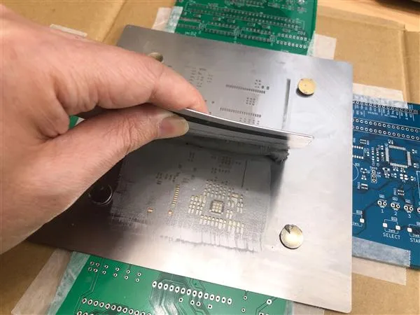
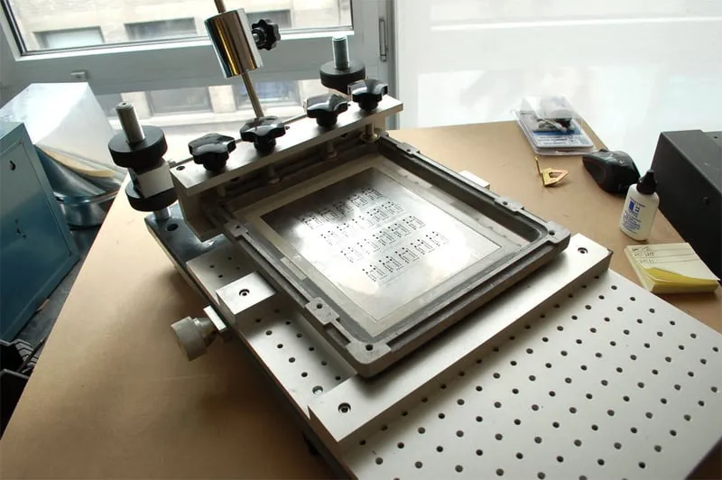
A high-quality PCB stencil is paramount in Surface Mount Technology (SMT) assembly, directly influencing the precision and consistency of solder paste deposition. This critical component ensures that the correct amount of solder paste is applied to the pads of a printed circuit board, thereby establishing reliable electrical connections during component mounting.
Inaccurate solder paste application, stemming from a poorly manufactured stencil, can lead to several defects such as solder bridges, insufficient solder, or component misalignment. These defects not only jeopardize the electrical functionality of the PCB but also impact the reliability of the final product, leading to increased failure rates and rework costs. Therefore, selecting a reliable stencil is not just a step in the manufacturing process but a crucial quality control measure.
Types of PCB Stencils: Comparing Options
Laser Cut Stencil
Selecting the appropriate PCB stencil is crucial for achieving precise solder paste deposition in SMT assembly. Different stencil types offer varying levels of performance, durability, and cost-effectiveness. This section details the most common options, including laser-cut stainless steel stencils, polyimide (Kapton) stencils, and the distinctions between framed and frameless designs.
Stencil Type
Material
Typical Applications
Advantages
Disadvantages
Laser-Cut Stainless Steel
Stainless Steel
High-volume production, fine-pitch components
High precision, durability, good paste release
Higher initial cost, less flexible
Polyimide (Kapton)
Polyimide Film
Prototypes, low-volume production, flexible PCBs
Flexibility, lower cost, good for fine-pitch components
Less durable, may require special handling
Framed Stencil
Various materials (typically stainless steel)
High-volume production, automated assembly
Consistent tension, easier handling in automated lines
Higher cost, requires storage space
Frameless Stencil
Various materials (typically stainless steel)
Low to medium volume production, manual assembly
Lower cost, requires less storage
More prone to damage, can be more difficult to use manually
Materials Used by PCB Stencil Manufacturers
Stainless Steel Stencil
The selection of materials for PCB stencils is crucial, directly influencing the stencil's performance, durability, and ultimately, the quality of solder paste application. Manufacturers primarily utilize stainless steel, brass, and polyimide (Kapton) for their specific properties. Understanding the characteristics of each material is vital for choosing the right stencil for a given application.
Material
Characteristics
Advantages
Disadvantages
Best Applications
Stainless Steel
High tensile strength, durable, resistant to corrosion, good dimensional stability.
Long lifespan, precise and consistent solder paste deposition, suitable for fine-pitch components.
More expensive than brass, may be susceptible to burrs without proper processing.
Most SMT applications, especially for high-volume production and fine-pitch components.
Brass
Softer than stainless steel, lower cost, easier to etch, good conductivity.
More affordable, good for prototyping and low-volume production, suitable for specific etching techniques.
Less durable than stainless steel, prone to bending and damage, less precise for fine-pitch.
Prototyping, low-volume production, and simpler circuit boards.
Polyimide (Kapton)
Flexible, low cost, can be easily laser cut, chemical resistant.
Cost-effective, good for flexible circuits, useful for specific adhesive applications.
Less durable and less precise than steel, may be prone to stretching and tearing.
Flexible PCBs, specialized adhesive printing, specific prototyping purposes.
Key Factors to Consider When Selecting a PCB Stencil Manufacturer
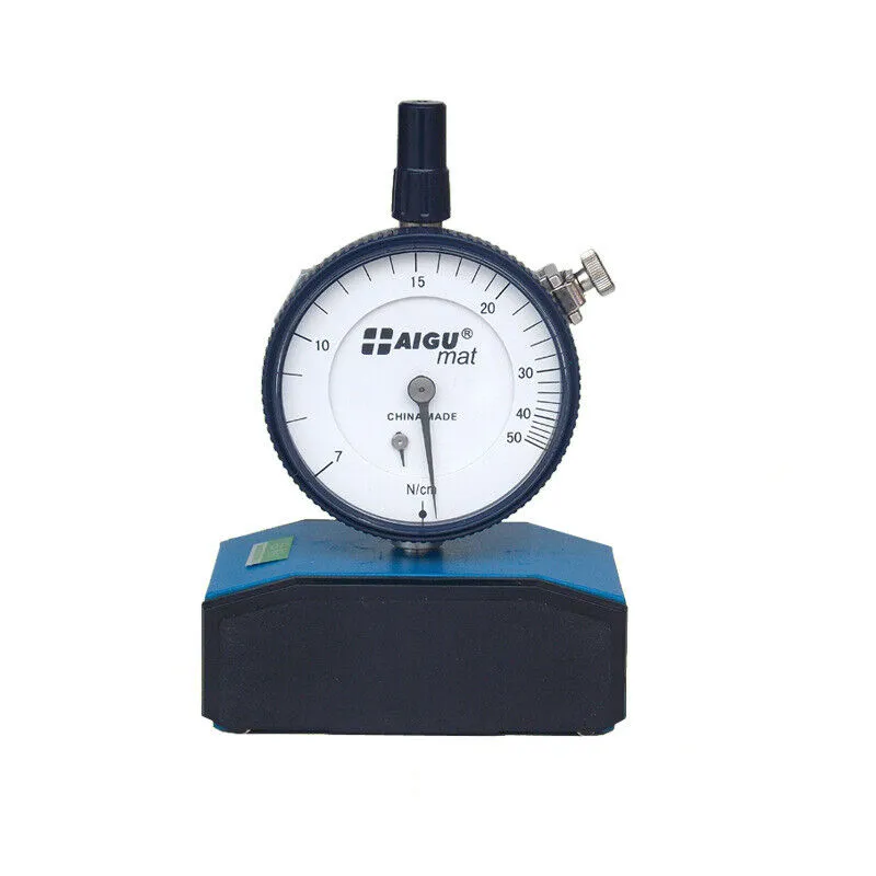
Stencil Tension Meter
Selecting the right PCB stencil manufacturer is crucial for the success of any surface mount technology (SMT) assembly project. Several key factors significantly impact the quality of the stencil, which in turn affects solder paste application, component placement accuracy, and ultimately, the reliability of the final product. Careful consideration of these factors will help ensure the manufacturer meets your specific needs and project requirements.
Factor
Description
Impact
Precision
The accuracy with which the stencil's apertures are cut, crucial for precise solder paste deposition.
Directly affects solder joint quality, preventing shorts, opens, and other assembly defects.
Turnaround Time
The time it takes for the manufacturer to produce and deliver the stencil.
Impacts project timelines and can cause delays in assembly if not managed well. Fast turnaround may incur additional costs.
Pricing
The cost of the stencil, which varies based on materials, complexity, and manufacturing techniques.
Influences overall project budget; balancing cost with required quality is essential. Be wary of extremely low prices as this may indicate lower quality.
Material Options
The range of materials available for stencil production such as stainless steel, brass, or polyimide.
Different materials have different properties, affecting durability, chemical resistance, and cost. Selecting the correct material for your application is critical.
Customer Support
The level of assistance provided by the manufacturer, including technical support, design advice, and responsiveness to inquiries.
Good customer support can help in resolving design and manufacturing issues, ensuring efficient and timely delivery of the finished stencils.
Evaluating the Technology and Manufacturing Process
Stencil Manufacturing Equipment
The precision and quality of a PCB stencil are heavily dependent on the technology and manufacturing processes employed by the manufacturer. A thorough evaluation of these aspects is crucial to ensure that the stencil meets the required specifications for accurate solder paste application and, ultimately, successful PCB assembly. This section details key elements to consider when assessing a manufacturer's capabilities.
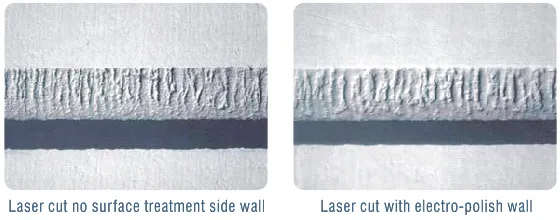
The core of stencil fabrication lies in laser cutting technology. High-precision laser cutting is paramount to achieving accurate aperture dimensions and smooth, burr-free edges. These factors directly influence the volume of solder paste deposited onto the PCB pads, ensuring consistent and reliable solder joints.
Laser Cutting Precision The laser cutting system should be capable of achieving tight tolerances on aperture dimensions, typically within a few microns. This accuracy ensures that the solder paste is deposited with the desired volume and shape, preventing shorts and opens during reflow soldering.
Quality of Edges The laser-cut edges should be clean, smooth, and free of burrs. Burrs or rough edges can interfere with the release of the solder paste from the stencil, leading to inconsistencies in solder deposition. High-quality laser cutting leaves a polished, smooth cut that facilitates proper solder paste release.
Material Handling The manufacturer's handling processes and equipment should also ensure that the stencil material is carefully managed and remains flat during the entire manufacturing process to eliminate warpage and maintain the precision of laser cuts
Quality Control Measures A robust quality control (QC) system is essential to verify that the manufactured stencils meet all specifications. This includes in-process inspections and post-manufacturing checks using high-resolution imaging systems, to ensure that the aperture dimensions and tolerances are accurate according to the design files, as well as to identify any defects or inconsistencies that may have occurred during the manufacturing process. Detailed inspection reports should be available.
Stencil Cleaning Processes The methods used to clean stencils post-fabrication directly affect their performance and longevity. Proper cleaning removes any residuals and contaminants, ensuring the stencil is ready for accurate solder paste deposition. The manufacturer should outline their cleaning methods and confirm they use the proper cleaning solutions that are compatible with their stencil material.
Frequently Asked Questions About PCB Stencils
This section addresses common queries regarding PCB stencils, providing concise answers to help clarify their function, value, and manufacturing process within the electronics assembly landscape. Understanding these basics is crucial for anyone involved in PCB design and manufacturing.
What is a PCB stencil and its role in manufacturing? A PCB stencil is a thin sheet of material, typically stainless steel, with precisely cut openings corresponding to the surface mount pads on a printed circuit board (PCB). Its primary function is to facilitate the controlled deposition of solder paste onto these pads, ensuring accurate and consistent solder joints during the SMT assembly process. It acts as a template, guiding the application of solder paste.
Are PCB stencils a necessary expense? Yes, for surface mount technology (SMT) assembly, PCB stencils are generally considered necessary. While they represent an upfront cost, stencils are crucial for achieving precise and repeatable solder paste application, which significantly reduces defects, improves reliability, and increases overall manufacturing efficiency. The cost of rework due to inadequate solder paste application far outweighs the cost of a quality stencil, ultimately making them a cost-effective investment for projects requiring SMT assembly.
How are PCB stencils typically manufactured? PCB stencils are predominantly manufactured using precision laser cutting. A laser beam is used to vaporize material along the desired pattern from a sheet of stainless steel or other specified material, resulting in the precise apertures required for solder paste deposition. This method ensures high accuracy and tight tolerances.
Can PCB stencils be reused, and how many times? Yes, PCB stencils are typically reusable. The number of times a stencil can be effectively reused depends on the material, storage, handling, and cleaning processes. Stainless steel stencils are generally more durable and can withstand multiple uses if handled correctly, often lasting for thousands of prints. Proper cleaning after each use is vital to ensure long-term usability and accuracy. Frame stencils are usually more durable for repeat use over their framed counterparts.
What are the different types of PCB stencils available? Common types of PCB stencils include laser-cut stainless steel stencils, which are the industry standard, offering precision and durability. Other types include polyimide (Kapton) stencils which are used for prototyping and flexible PCBs where there is a need for some flexibility in the stencil and also chemically etched stencils, which are typically the least accurate and lowest cost. Stencils are also categorized as framed or frameless depending on whether they are mounted on a frame or directly used on the PCB assembly equipment.
What does stencil thickness mean? Stencil thickness refers to the height of the stencil material used, and it directly impacts the amount of solder paste deposited on the PCB pads. Thicker stencils release more solder paste, which may be needed for larger components, while thinner stencils are better suited for fine-pitch components to prevent solder bridging. Selecting the correct thickness is critical for achieving the desired solder volume and quality.
How does stencil aperture design influence the solder paste application? The design of the openings (apertures) in a PCB stencil is crucial for proper solder paste deposition. Aperture shape and size need to match the size and layout of the pads on the PCB, and is also impacted by the size of the paste being used. Stencil manufacturers may modify the aperture shape or size in order to improve solder paste release. This consideration of design allows for optimum paste release and correct solder joint formation.
Comparing PCB Stencil Manufacturers: A Checklist
Stencil Comparison
Selecting the right PCB stencil manufacturer is crucial for ensuring high-quality surface mount assembly. This checklist provides key criteria for evaluating potential manufacturers, helping you make informed decisions based on your project's specific needs and budgetary constraints. By systematically assessing these factors, you can minimize risks and achieve optimal results in your PCB assembly process.
Precision and Accuracy Verify the manufacturer’s capabilities for achieving the required precision in stencil apertures. Look for specifications regarding laser cutting accuracy, positional tolerance, and aperture size control. Precision directly impacts solder paste deposition and component placement.
Material Options Ensure the manufacturer offers a range of materials, including stainless steel (different grades), brass, and polyimide (Kapton). Consider the material's durability, chemical resistance, and suitability for your project's requirements and production volume.
Manufacturing Process Evaluate the manufacturer's laser cutting process and quality control measures. Precision laser cutting is essential for achieving accurate aperture dimensions, sharp edges, and smooth walls. Confirm the utilization of automated inspection methods.
Turnaround Time Assess the manufacturer’s quoted lead times for stencil production and delivery. Inquire about any rush order options and their associated costs. This is particularly critical for time-sensitive projects where delays can significantly impact schedules.
Pricing and Cost Structure Request detailed quotes that outline all costs including stencil design, material selection, manufacturing, and any post-processing or inspection costs. Compare quotes from different manufacturers and understand any volume discounts available.
Customer Support and Communication Gauge the manufacturer’s responsiveness and communication skills. It is crucial they provide prompt, clear, and helpful support, as this plays a role in ensuring project requirements are accurately conveyed and issues are resolved promptly.
Stencil Framing Options Check whether the manufacturer can provide framed, frameless, or prototype stencils and what options they offer regarding tensioning. Framed stencils are typically better for high volume production whilst frameless stencils can be advantageous from a cost and storage perspective for prototypes and short production runs.
Cost-Effective Solutions for PCB Stencil Manufacturing
Bulk Stencils
Optimizing costs in PCB stencil manufacturing is crucial for efficient budget management without sacrificing quality. Several strategies can be implemented to achieve this balance, focusing on material selection, design optimization, and supplier negotiation.
Standardize Design Adopting standardized designs allows manufacturers to streamline the stencil fabrication process, reducing setup time and material waste. Common fiducial marks and consistent panel sizes across different PCB designs can significantly lower manufacturing costs and improve production efficiency.
Optimize Material Usage Choosing the correct thickness for a stencil to match the needs of the surface-mounted components can reduce the cost and waste of solder paste. Additionally, if only the highest precision is needed for a part of the panel, a hybrid design with a more cost-effective material for the less demanding parts can be considered to lower overall cost.
Negotiate with Suppliers Establishing long-term relationships with reliable PCB stencil manufacturers can lead to favorable pricing agreements and volume discounts. It is advantageous to discuss with the supplier to find the best process for the project’s need. This approach can be particularly effective for ongoing projects or for large orders.
Consider Frameless Stencils Frameless stencils generally come at a lower cost compared to framed stencils. While they require a tensioning system, for large-scale projects, their reusability and reduced storage space requirements can lead to long-term cost savings. This is particularly relevant for high volume production environments.
Combine Orders Consolidating multiple stencil orders into larger batches often reduces per-unit costs. This is beneficial for companies that may have varying but simultaneous production requirements. By planning ahead and placing combined orders, significant savings can be achieved through economies of scale.
Cost Optimization Strategy
Description
Impact on Cost
Standardize Design
Use common fiducials, panel sizes
Reduced set-up time and waste
Optimize Material Usage
Match stencil thickness to project needs
Reduced material waste
Negotiate with Suppliers
Long-term agreements, volume discounts
Lower unit costs
Consider Frameless Stencils
Reusable, less storage
Lower long-term costs
Combine Orders
Larger batches
Economies of scale
Choosing the right PCB stencil manufacturer is an important decision impacting the success of any SMT assembly project. Understanding the available options, materials, manufacturing process, and considering factors such as precision and cost are crucial steps. Whether you are looking for a prototype stencil or a high-volume solution, carefully weighing your options will ensure you partner with the best PCB stencil manufacturer who provides high-quality and reliable stencils to meet your needs, leading to successful assembly outcomes and ultimately the success of the end product.