In the age of ever-evolving technology, Printed Circuit Boards (PCBs) are the unsung heroes powering our devices. JLCPCB factory stands at the forefront of this industry, transforming raw materials into the fundamental building blocks of modern electronics. This article will take you behind the scenes, exploring the sophisticated processes employed at JLCPCB and shedding light on how they ensure precision, efficiency, and affordability in PCB manufacturing and assembly.
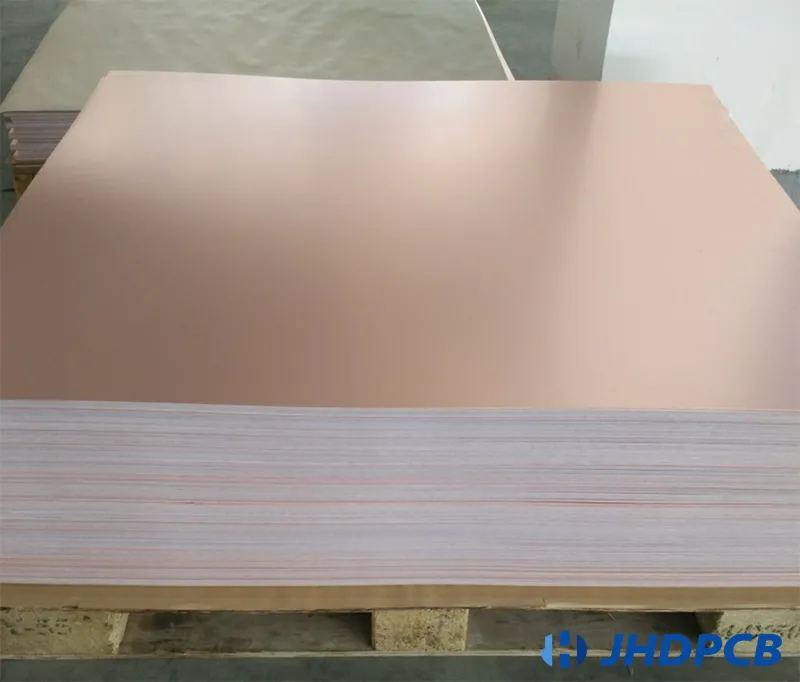
The initial phase of PCB manufacturing at JLCPCB is characterized by the meticulous selection and preparation of raw materials. This crucial step ensures the foundation for high-quality circuit boards. JLCPCB employs a variety of materials, including different grades of laminates, copper foils, and other specialized materials, each chosen for their specific performance characteristics and adherence to industry standards. Proper storage and handling protocols are strictly followed to maintain material integrity and prevent contamination, thus laying the groundwork for consistent and reliable PCB production.
| Material Type | Common Variants | Typical Application | Key Properties |
|---|---|---|---|
| Laminates | FR-4, CEM-1, Polyimide | Core PCB substrate | Mechanical strength, dielectric constant, thermal resistance |
| Copper Foil | 1/2 oz, 1 oz, 2 oz | Conductive layer for circuits | Conductivity, thickness, adhesion |
| Prepreg | Various resin content | Insulating layers between copper layers | Dielectric strength, resin flow |
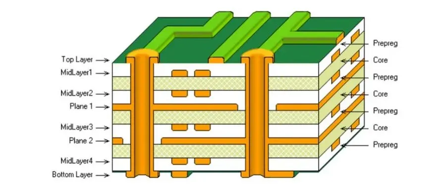
The transformation of raw materials into functional printed circuit boards (PCBs) at JLCPCB is a meticulously controlled multi-stage process. This section details the core steps involved in PCB fabrication, including imaging, etching, and lamination, which are fundamental to achieving the desired circuit patterns and overall board structure.
| Process | Description | Purpose | Equipment |
|---|---|---|---|
| Imaging | Transferring circuit pattern onto resist using UV light | Defines the areas to be etched | Photo plotter, UV exposure unit |
| Etching | Chemical removal of unprotected copper | Creates the conductive traces | Etching machines, chemical baths |
| Lamination | Bonding multiple layers using heat and pressure | Forms multi-layer board structure | Lamination press, precise temperature control system |
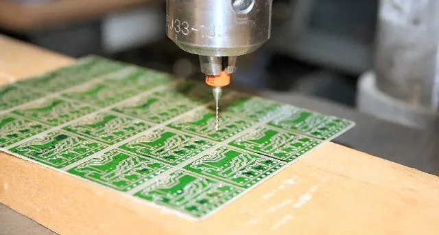
The creation of precise holes and vias is paramount in PCB fabrication, enabling electrical connections between different layers of the board. JLCPCB utilizes state-of-the-art automated drilling equipment to ensure accuracy and efficiency in this critical process.
Drilling and via formation are not merely about making holes; they involve precision engineering, controlling hole diameter, plating quality, and alignment. JLCPCB employs computer-controlled drilling machines that can execute complex drilling patterns with high repeatability.
| Parameter | Description | Value |
|---|---|---|
| Minimum Drill Hole Size | Smallest diameter of hole that can be drilled | 0.15mm |
| Drill Accuracy | Precision of the hole placement | +/- 0.05mm |
| Via Plating Material | Material used for plating vias | Copper |
| Drilling Capacity | Number of holes that can be drilled per unit time | Variable, dependent on board complexity |
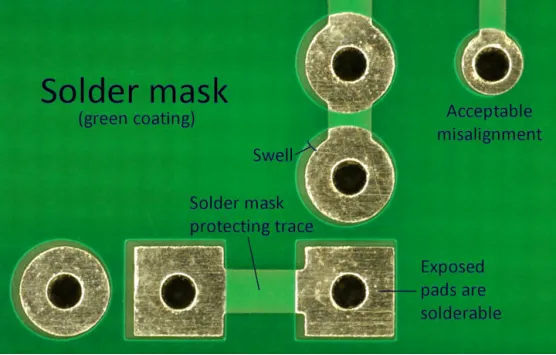
Solder mask application and surface finishing are critical steps in PCB manufacturing at JLCPCB, ensuring both the functional integrity and longevity of the boards. The solder mask acts as a protective layer, preventing solder bridges during assembly, while surface finishing enhances solderability and protects exposed copper from oxidation.
These processes are essential for achieving reliable performance and are carefully controlled by JLCPCB using state-of-the-art equipment and meticulous procedures.
| Process | Description | Purpose | Materials | Equipment |
|---|---|---|---|---|
| Solder Mask Application | Application of a thin polymer layer over the PCB substrate, except for areas designated for soldering. | Prevents solder bridges and protects tracks; determines where components can and can't be soldered. | Epoxy-based or acrylic-based photosensitive solder mask ink. | Automated screen printing or spray coating machines with UV curing systems. |
| Surface Finishing | Application of a metallic coating over exposed copper pads and vias. | Enhances solderability, prevents copper oxidation, improves electrical conductivity. | Electroless Nickel Immersion Gold (ENIG), Hot Air Solder Leveling (HASL), Immersion Tin, Immersion Silver, Organic Solderability Preservatives (OSP). | Automated plating lines, chemical baths, reflow ovens. |
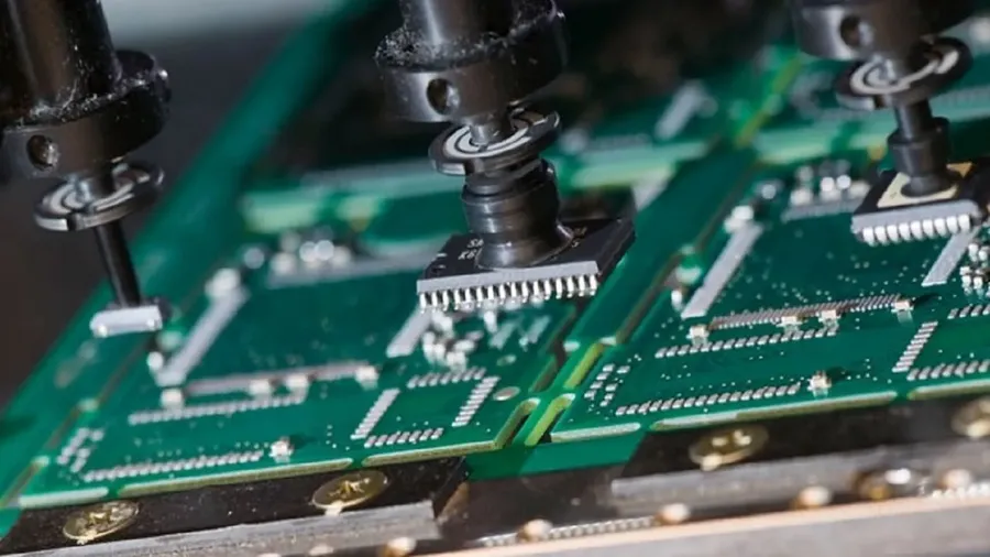
The component placement stage in PCB assembly at JLCPCB is a highly automated process, crucial for achieving both precision and high-volume production. This stage involves the accurate and rapid placement of electronic components onto the bare printed circuit boards using both Surface Mount Technology (SMT) and through-hole techniques, setting the stage for subsequent soldering and testing. JLCPCB utilizes advanced pick-and-place machines equipped with vision systems and precise robotics to ensure accurate component positioning.
| Technology | Description | Components | Placement Method | Typical Applications |
|---|---|---|---|---|
| Surface Mount Technology (SMT) | Components are directly mounted onto the surface of the PCB. | Resistors, capacitors, integrated circuits (ICs), LEDs | Automated pick-and-place machines with vacuum nozzles. | High-density designs, consumer electronics, portable devices. |
| Through-Hole Technology (THT) | Components have leads that are inserted through drilled holes on the PCB. | Connectors, switches, large capacitors, inductors. | Manual insertion, automated assembly for specific components. | Power supplies, high-current applications, robust mechanical connections. |
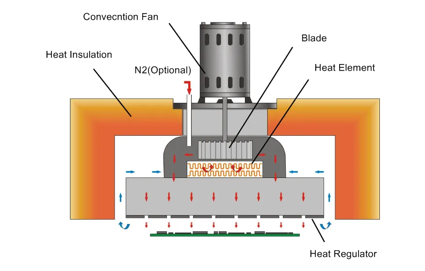
Reflow soldering is a critical process at JLCPCB, ensuring components are permanently and reliably attached to the PCB. This step is followed by rigorous quality control measures to guarantee that every board meets stringent performance and reliability standards.
The reflow soldering process is meticulously controlled to ensure optimal solder joints, which are essential for the electrical and mechanical integrity of the final product. JLCPCB employs advanced techniques and equipment to manage this delicate balance.
| Process Stage | Description | Key Parameters | Quality Control Focus |
|---|---|---|---|
| Solder Paste Application | Precision deposition of solder paste onto PCB pads. | Volume, alignment, and paste viscosity | Ensuring consistent and accurate placement |
| Component Placement | Automated placement of surface mount components onto the solder paste. | Component alignment and pressure | Verifying correct component orientation and position |
| Reflow Soldering | Controlled heating of the PCB to melt the solder paste and form permanent connections. | Temperature profile, ramp rate, and peak temperature. | Precise temperature management to avoid cold solder joints or overheating components |
| Post-Solder Inspection | Visual and automated inspection of solder joints. | Visual and X-ray inspection parameters | Detecting defects such as shorts, opens, or insufficient solder |
Quality control at JLCPCB is an integral part of the manufacturing process. It involves multiple stages from initial inspection of raw materials to final board verification. This multi-layered approach ensures that each PCB produced adheres to the highest standards of quality and reliability.
JLCPCB distinguishes itself through its adept handling of complex PCB designs, going beyond standard single and double-layer boards to provide multi-layer, flexible, and other specialized PCB solutions. The company's commitment to advanced technologies ensures they meet the evolving needs of modern electronics, from simple consumer devices to intricate industrial and aerospace applications.
This section explores these advanced capabilities, detailing how JLCPCB maintains its position at the cutting edge of PCB manufacturing.
| Technology | Description | JLCPCB Capabilities |
|---|---|---|
| Multi-layer PCBs | Boards with more than two conductive layers, enabling increased circuit complexity and component density. | Up to 20 layers standard production, with more on request. Precise layer registration and impedance control. |
| Flexible PCBs (FPC) | Boards built on flexible substrates that can bend and fold. Ideal for tight spaces and dynamic applications. | Single and multi-layer flexible PCBs. Wide range of material options, and specialized surface finishes. |
| HDI PCBs | High-Density Interconnect PCBs, characterized by finer lines, micro vias, and high component density. | Micro vias, fine pitch circuits, laser drilling, sequential lamination for advanced device integration. |
| Metal Core PCBs | Boards with a metal core, for excellent heat dissipation properties. | Various metal core materials like aluminum and copper, thickness options, and thermal management solutions. |
| Specialized Surface Finishes | Surface plating and finishes that improve solderability, protect from corrosion, and enhance signal integrity. | ENIG, HASL, Immersion Tin, Immersion Silver, and OSP for different application requirements. |
| Blind and Buried Vias | Vias that connect layers internally without going through all layers. | Advanced drilling and via formation techniques that enhance routing density, signal integrity. |
JLCPCB leverages cutting-edge manufacturing equipment and a robust research and development team to continuously improve its process and incorporate new technologies. This commitment to innovation allows them to meet the diverse and demanding requirements of their global customer base, ensuring quality and performance for every manufactured PCB.
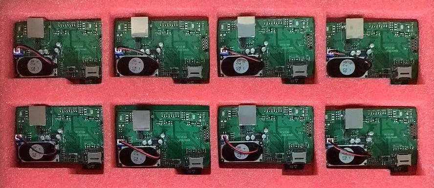
JLCPCB provides flexible options for receiving your manufactured PCBs, including both factory pick-up for local clients and various global shipping methods. This ensures that clients can choose the most efficient and cost-effective way to receive their orders.
This section addresses common queries regarding JLCPCB's operations, manufacturing capabilities, and logistical considerations. We aim to provide clear and concise answers to assist users in understanding JLCPCB's role in the global PCB manufacturing landscape.
The JLCPCB factory demonstrates a commitment to precision and efficiency in PCB manufacturing and assembly. Their use of automated processes, coupled with rigorous quality control, ensures the delivery of high-quality PCBs to meet the diverse needs of the global electronics industry. From raw material handling to final shipping, JLCPCB is a model of modern, cutting-edge PCB production. JLCPCB's continuous innovation and dedication to excellence positions them as a key player in the future of electronics. By showcasing the inner workings of the factory, we've highlighted the technological sophistication and commitment that underpin every circuit board produced.

