Comprehensive Guide to PCB Assembly: From Design to Final Product
2025.01.20
In the intricate world of electronics, the Printed Circuit Board (PCB) stands as the foundational platform, much like the skeletal system of the human body. PCB assembly is the process of mounting electronic components onto a PCB. This seemingly simple act is where theory meets reality, transforming a designed schematic into a functional electronic device that impacts our lives daily. This article will delve deep into the world of PCB assembly, demystifying its complex processes and providing valuable insights for enthusiasts and professionals alike, from initial design to final product testing.
Understanding PCB Assembly: An Overview
Assembled PCB
Printed Circuit Board Assembly (PCBA) is the crucial process of mounting electronic components onto a fabricated PCB, transforming it from a bare board into a functional electronic module. This process is distinct from PCB fabrication, which involves creating the conductive traces and layers of the board. PCBA is paramount in electronics manufacturing, as it dictates the final functionality and performance of the electronic device.
The distinction between PCB fabrication and PCB assembly is essential: fabrication creates the 'canvas,' while assembly places the 'artwork' (components) onto it. The functionality of any electronic product heavily relies on the precision and accuracy of the PCB assembly process. A poorly assembled PCB will result in a non-functional or unreliable device, regardless of the quality of the original design or the individual components used.
Key Steps in the PCB Assembly Process
SMT Placement
The PCB assembly process, a critical stage in electronics manufacturing, involves a series of precise steps to transform a bare printed circuit board into a functional electronic assembly. These steps, which range from solder paste application to final inspection, are crucial for ensuring the reliability and performance of the end product.
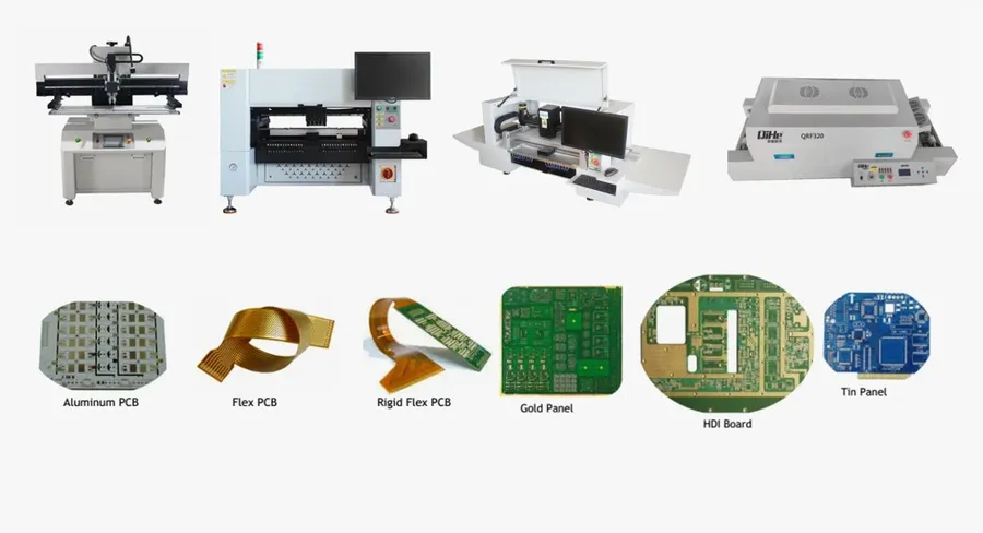
Solder Paste Application The process begins with the precise application of solder paste onto the PCB pads using a stencil. Solder paste, a mixture of solder particles and flux, ensures effective solder connections during reflow. The method of application—stencil printing or jet dispensing—depends on the complexity and density of the board.
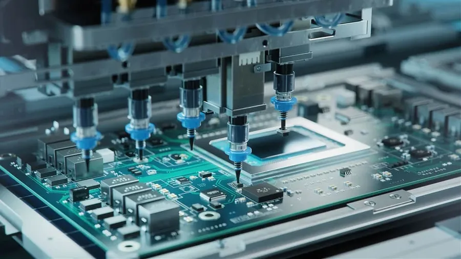
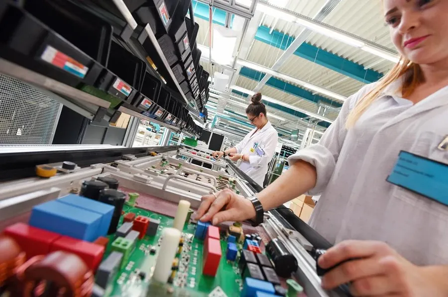
Component Placement Following solder paste application, components are accurately positioned onto the board. This phase includes both Surface Mount Technology (SMT) component placement, using pick-and-place machines, and through-hole component insertion either manually or through automated equipment. Precise placement is crucial for functionality.
Reflow Soldering The assembled board then proceeds to a reflow oven. Here, controlled heating melts the solder paste, forming permanent electrical connections between components and the PCB. The temperature profile must be carefully managed to ensure strong solder joints without damaging components.
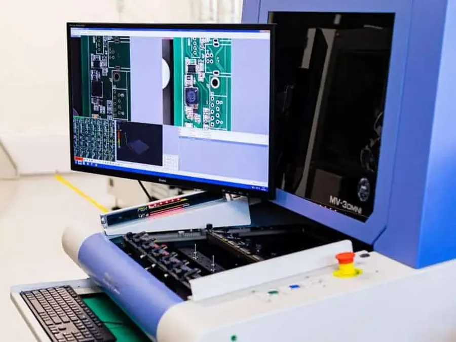
Inspection Post-soldering, rigorous inspection is conducted. This includes visual inspection, Automated Optical Inspection (AOI), and potentially X-ray inspection. These checks are vital for identifying defects like solder bridges, component misalignment, and insufficient solder, guaranteeing the high quality of the assembled PCB.
Surface Mount Technology (SMT) vs. Through-Hole Assembly
Through-Hole PCB
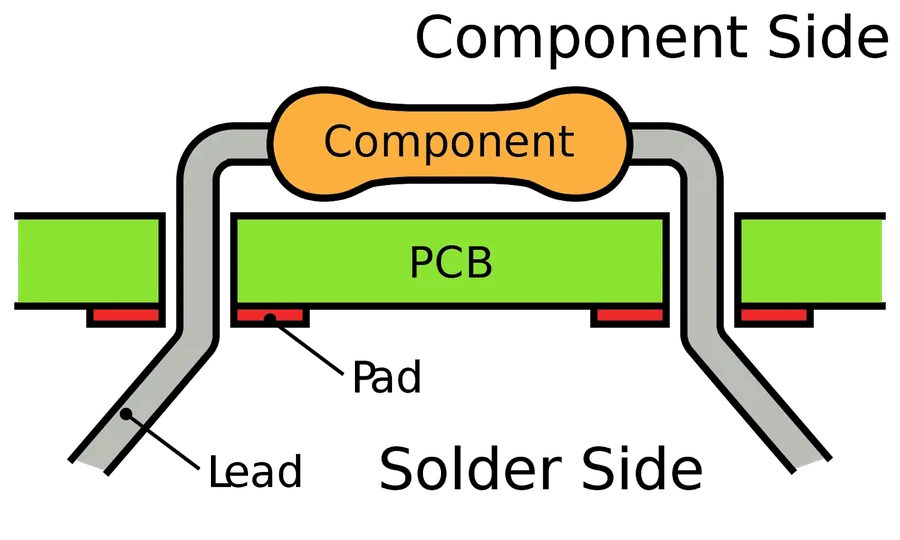
Printed circuit board (PCB) assembly employs two primary component mounting techniques: Surface Mount Technology (SMT) and Through-Hole Technology. The selection between these methods is crucial and significantly impacts the final product's performance, cost, and manufacturability. SMT involves placing components directly onto the PCB surface, while through-hole assembly entails inserting component leads through holes in the board and soldering them on the opposite side.
Feature
Surface Mount Technology (SMT)
Through-Hole Technology
Component Mounting
Components are placed directly on the PCB surface.
Component leads are inserted through holes in the PCB and soldered on the opposite side.
Component Size
Typically uses smaller, miniaturized components.
Components are typically larger with leads or pins.
Component Density
Allows for higher component density on the board.
Lower component density due to spacing requirements.
Assembly Process
Automated process suitable for high-volume production.
Manual or semi-automated process often used for prototyping and low-volume production.
Cost
Generally more cost-effective for high-volume production due to automation.
Can be more expensive due to manual labor in low-volume runs and larger components.
Mechanical Strength
Components are less mechanically robust and susceptible to damage under stress or vibration.
Components are more mechanically robust and resistant to damage under stress or vibration.
Repair and Modification
More challenging to repair or modify.
Easier to repair or modify components
Applications
Widely used in consumer electronics, mobile devices, and other high-density applications.
Commonly used in applications requiring high mechanical strength, such as power supplies and connectors.
Choosing between SMT and through-hole technology depends on a variety of factors such as production volume, performance requirements, and cost constraints. Often, a design will incorporate both SMT and through-hole components, taking advantage of the benefits of each method. SMT is often preferred for high-volume, compact designs due to its cost-effectiveness and density, whereas through-hole is chosen for larger, more robust components that require stronger connections. The careful consideration of these factors will determine the optimum approach for PCB assembly.
Design for Assembly (DFA) Guidelines for PCB Assembly
PCB Design Layout
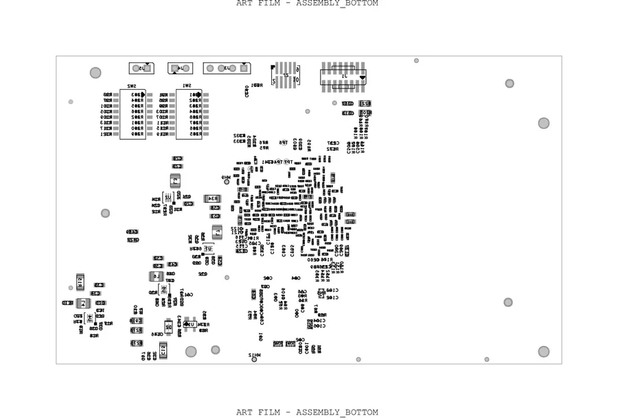
Design for Assembly (DFA) is a crucial methodology in PCB assembly that focuses on optimizing the design of a printed circuit board to facilitate efficient, cost-effective, and reliable manufacturing. By integrating DFA principles into the design phase, manufacturers can significantly reduce assembly time, minimize errors, and enhance the overall quality of the final product. This involves careful consideration of component placement, orientation, spacing, and the selection of materials.
Component Placement and Orientation Strategic placement of components, with attention to polarity and orientation, is paramount for automated assembly processes. Components should be aligned to minimize rotation and movement during placement. Consistent orientation is also key to streamline inspection and testing.
Spacing and Clearance Rules Adequate spacing between components and board features such as fiducial markers and edge rails, is crucial for preventing collisions during automated assembly. Proper clearances also ensure sufficient space for soldering tools to prevent damage to neighboring components and to facilitate effective inspection.
Fiducial Markers The inclusion of fiducial markers enables pick-and-place machines to accurately align the PCB, ensuring precise component placement. Global and local fiducials are essential for accurate assembly.
Panelization When creating a panel for manufacturing, ensure that all individual circuit boards are separated by the correct spacing and that no individual circuit board has a part that is on the border. This will increase throughput and help the assembly partner avoid issues when depanelizing the boards.
Component Selection Choosing standard package components simplifies assembly. Utilizing components from the same manufacturer where possible simplifies pick and place as the component tape and reel can be used with out need to change reels on the production line, which reduces the total production time. Components should also be chosen based on their soldering profile and manufacturability.
Avoidance of Difficult to Manufacture Components Complex or unstandard components are harder to place, may require extra steps and may not be readily available. These extra challenges will result in increased costs and production time.
Solder Pad Design Solder pad design is critical for proper soldering. Ensure that pad sizes are appropriate for the components being used, which includes the solderable surface and stencil aperture size. Incorrect pad sizes can lead to solder bridges, opens, and other defects.
PCB Assembly Quality Control and Inspection
AOI Inspection Machine
Rigorous quality control and inspection are paramount in PCB assembly (PCBA) to ensure the reliability and performance of the final product. These processes identify defects introduced during manufacturing, preventing costly failures and ensuring adherence to design specifications. A multi-faceted approach, combining visual, automated, and specialized inspection techniques, is critical for achieving consistently high-quality assemblies.
Inspection Method
Description
Advantages
Disadvantages
Visual Inspection
Manual examination of PCBs using microscopes and magnifying glasses.
Cost-effective, good for detecting gross defects.
Subjective, time-consuming, prone to human error, not suitable for fine-pitch components.
Automated Optical Inspection (AOI)
Automated system using cameras and image processing to detect defects.
Fast, objective, suitable for high-volume production, can detect a wide range of defects.
Can be expensive to set up, may require fine-tuning for different PCB designs, may not detect all types of defects.
X-Ray Inspection
Uses X-rays to examine the internal structure of the PCB and solder joints.
Effective for detecting hidden defects like solder voids, BGA solder joint issues, and internal layer misalignments.
Expensive, may not be suitable for all types of boards.
In-Circuit Testing (ICT)
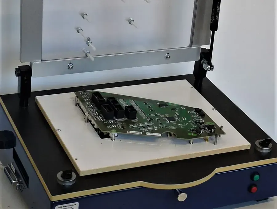
Uses test fixtures and electrical probes to test for shorts, opens, and component functionality.
Highly accurate for electrical functionality testing
Requires a dedicated test fixture, may not catch defects related to component placement or solder quality.
The Importance of Testing in PCB Assembly
PCB Functional Test
Rigorous testing is paramount in PCB assembly to validate the correct fabrication and functionality of the assembled printed circuit boards (PCBAs). Testing ensures that the final product meets design specifications and performance requirements, thereby preventing costly failures and recalls after deployment.
Several testing methodologies are employed, each designed to identify different types of defects and verify specific aspects of the PCBA's operation. These methodologies can be broadly categorized into functional testing and in-circuit testing (ICT), supplemented by other specialized tests as required.
Testing Method
Purpose
Process
Advantages
Disadvantages
Functional Testing
Verifies the overall functionality of the assembled PCB.
Simulates the intended operating conditions and checks if the PCBA performs as designed.
Tests the integrated system, covering all components and their interactions.
May not pinpoint specific component-level faults; time-consuming setup for new designs.
In-Circuit Testing (ICT)
Checks for component and solder joint defects on the PCB.
Uses a bed-of-nails fixture to probe specific test points on the board to check circuit parameters.
Quick detection of component shorts, opens, and wrong values.
Expensive setup for bed-of-nails fixtures; less effective for complex circuits with many components.
X-ray Inspection
Inspects solder joints and internal component structures.
Uses X-rays to penetrate components and observe solder quality, voiding, and hidden defects.
Detects defects not visible to the human eye; evaluates ball grid array (BGA) solders.
High equipment cost; may not show minor faults, and requires skilled operators.
Automated Optical Inspection (AOI)
Visually inspects for defects, such as component misplacement and solder joint issues.
Uses cameras to capture images and compare them against a set standard, to identify any discrepancies.
Faster inspection speed, good for detecting many types of defects; relatively lower cost.
May not detect defects under components, or some smaller soldering issues.
The selection of testing methods often depends on factors such as complexity of the PCBA, the production volume, and the application requirements of the final product. A multi-faceted approach utilizing a combination of these testing methodologies ensures the highest level of reliability and performance in PCB assemblies.
Common Challenges in PCB Assembly and How to Avoid Them
PCB assembly, while a sophisticated process, is susceptible to various challenges that can compromise the quality and functionality of the final product. Addressing these issues proactively through meticulous planning and execution is paramount to successful manufacturing.
Soldering Defects Issues like solder bridges, cold joints, and insufficient solder can lead to poor electrical connections and circuit malfunction. Prevention involves careful control of solder paste application, reflow oven temperature profiles, and regular maintenance of soldering equipment.
Component Misplacement Components not placed accurately on the PCB can result in short circuits, open circuits, and functional failures. Accurate pick-and-place machines, coupled with thorough component orientation checks and proper fiducial mark usage are crucial to avoiding component misplacement.
Tombstoning Also known as the Manhattan effect, tombstoning occurs when one end of a component lifts from the solder pad during reflow soldering. This is primarily due to uneven solder melting which pulls the component to one side. Prevention strategies include ensuring balanced thermal pads, optimal component orientation and consistent solder paste volume.
Solder Balling Solder balling refers to small solder spheres that separate from the solder paste during reflow. These balls can cause shorts if they land in unintended areas. Causes include excess moisture in the solder paste, improper reflow temperature profiles, or excessive preheating. Implementing correct storage, and correct heating parameters are important to reduce the incidence of solder balling.
Insufficient Paste Volume Insufficient solder paste application can result in weak or unreliable solder joints. Correct paste stencil design and precise application techniques are important to achieve the correct solder paste volume.
Incorrect Component Orientation Even with correct placement, incorrect component orientation can lead to a dysfunctional circuit. This can be avoided through visual checks and by using polarized component markings.
Poor PCB Handling Practices Mishandling PCBs can cause physical damage, contamination, and electrostatic discharge. Utilizing proper handling equipment, anti-static materials and following the correct PCB storage procedures is critical to preventing damage during assembly.
Component Obsolescence Components becoming obsolete can disrupt the production process and increase costs. Consistent review of component lifecycle and implementing alternative sourcing strategies can help mitigate this risk.
Frequently Asked Questions About PCB Assembly
This section addresses common questions surrounding PCB assembly, providing clear and concise answers to enhance understanding of this crucial process in electronics manufacturing.
What exactly is PCB Assembly (PCBA)? PCB assembly (PCBA) refers to the process of mounting electronic components onto a printed circuit board (PCB). This involves placing and soldering components such as resistors, capacitors, integrated circuits, and connectors onto the bare board, transforming it into a functional electronic circuit.
What does PCB stand for? PCB stands for Printed Circuit Board. It's the foundation upon which electronic components are mounted and connected to form an electronic circuit. The board provides mechanical support and electrical pathways (traces) for the components.
What is the role of a PCB Assembly? The role of a PCB assembly is to provide a reliable platform for electronic components to interact and perform intended functions. It ensures all components are correctly connected and supported, and that electrical signals are conducted accurately, enabling the desired operation of the electronic device.
Why can PCB assembly be expensive? The cost of PCB assembly is influenced by several factors including the complexity of the board design, the number of components, the type of components, the required assembly technology (SMT or through-hole), and the level of quality control and testing. Small-batch and high-precision assemblies are generally more expensive due to setup and labor costs.
What is the difference between PCB fabrication and PCB assembly? PCB fabrication involves the manufacturing of the bare circuit board itself, with the copper traces and other features created on the substrate. PCB assembly, on the other hand, is the subsequent process of placing and soldering electronic components onto this fabricated board.
How can I ensure high quality in my PCB Assembly? High quality in PCB assembly is achieved through strict adherence to design specifications, careful selection of components, proper execution of assembly processes (solder paste application, component placement, reflow soldering), thorough inspection (visual, AOI, X-ray), and comprehensive testing (functional, ICT). It is essential to partner with experienced assembly providers.
What are some common PCB assembly defects and how to avoid them? Common defects include soldering issues like solder bridges and cold solder joints, component misplacement, incorrect orientation, and board contamination. Prevention involves meticulous planning, stringent process controls, careful handling of components, and thorough inspection at each stage.
Choosing a PCB Assembly Partner: Factors to Consider
PCB Assembly Factory
Selecting the right PCB assembly partner is crucial for ensuring the quality, reliability, and cost-effectiveness of your electronic products. This section outlines the key factors to consider when choosing a PCB assembly service, helping you make an informed decision that aligns with your project requirements and business goals.
When evaluating potential PCB assembly partners, consider these factors:
Cost Evaluate not only the unit price, but also tooling costs, NRE charges, and potential costs associated with revisions. A low initial quote might hide additional expenses later in the process. Understand the full cost structure including payment terms, shipping, and customs.
Lead Time Assess the partner's lead time capabilities in relation to your project timeline. Ensure the partner's stated lead time aligns with your deadlines. Inquire about rush order options and associated costs, if needed, and consider variability in lead times given supply chain issues.
Production Capacity Confirm their ability to handle your production volumes. Can they scale up for future needs? Assess their manufacturing capabilities such as surface mount technology (SMT) and through-hole technology, assembly line automation, and material handling capacity.
Technical Expertise Evaluate the partner's experience with different board types, component complexities, and specific industry standards. Inquire about their technical capabilities, engineering expertise, and design for manufacturability (DFM) input.
Quality Assurance and Certifications Verify the partner's quality control processes and certifications (e.g., ISO 9001, IPC standards). What inspection methods do they use? How do they handle defects? Look for evidence of robust quality management systems and continuous improvement processes. Confirm the compliance with international safety, environmental and industry standards.
Communication and Customer Support Evaluate their responsiveness and communication style. A responsive and proactive partner can significantly simplify the project management process. Look for clear points of contact, project tracking options, and efficient communication channels.
Location and Logistics Consider geographical location as this impacts communication and shipping times. Understand the supplier's logistical capabilities including handling and transportation. Factor in any costs and issues related to international customs, lead time and transportations.
Ultimately, selecting the best partner involves a detailed analysis of these factors, aligning them with the specific needs of your project, and taking a long-term view to establish a relationship with a partner that will support your business growth and production needs. A well-chosen partner will not only manufacture your boards but also serve as a vital contributor to the success of your product.
In conclusion, PCB assembly is a critical process in electronics manufacturing that requires precise planning, execution, and quality control. From initial design considerations to the final testing stages, each step plays an important role in the creation of reliable and efficient electronic devices. By understanding the intricacies of PCB assembly, both hobbyists and professionals can navigate this world with greater confidence, innovation, and ultimately deliver better products. The future of electronics will continue to depend on the advancements of PCB assembly techniques and technologies.