In today's data-driven world, the ability to accurately and efficiently acquire data is paramount across various industries, from scientific research to industrial automation. At the heart of any data acquisition system lies the Printed Circuit Board (PCB), the unsung hero responsible for signal integrity, power distribution, and overall system performance. But what exactly constitutes a high-quality PCB solution for data acquisition instruments, and how can it impact your project's success? Join us as we delve deep into the world of Data Acquisition Instrument PCB Solutions, exploring the key considerations, design intricacies, and manufacturing best practices that Zero One Solution Limited brings to the table.
Introduction to Data Acquisition Instrument PCBs
Data Acquisition Instrument
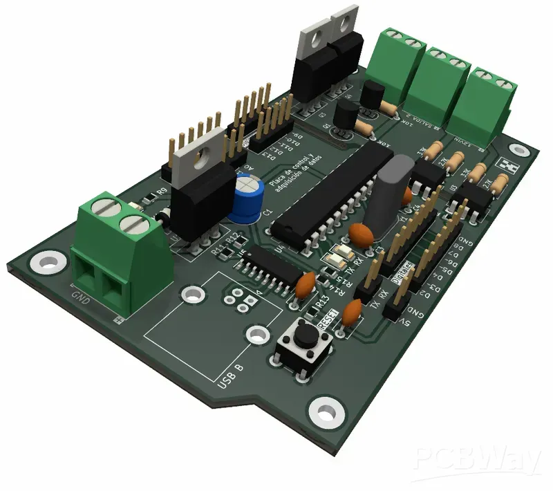
Data Acquisition (DAQ) instruments are the unsung heroes of modern technological advancement, serving as the critical bridge between the physical world and digital analysis. These sophisticated devices convert real-world analog signals—such as temperature, pressure, voltage, and current—into digital data that computers can process, store, and analyze. The Printed Circuit Board (PCB) at the core of a DAQ instrument is not merely a component carrier; it is the central nervous system, dictating the precision, speed, and reliability of data capture. Its design profoundly impacts signal integrity, noise immunity, and overall system performance, making it a pivotal element in applications ranging from scientific research and industrial automation to medical diagnostics and environmental monitoring.
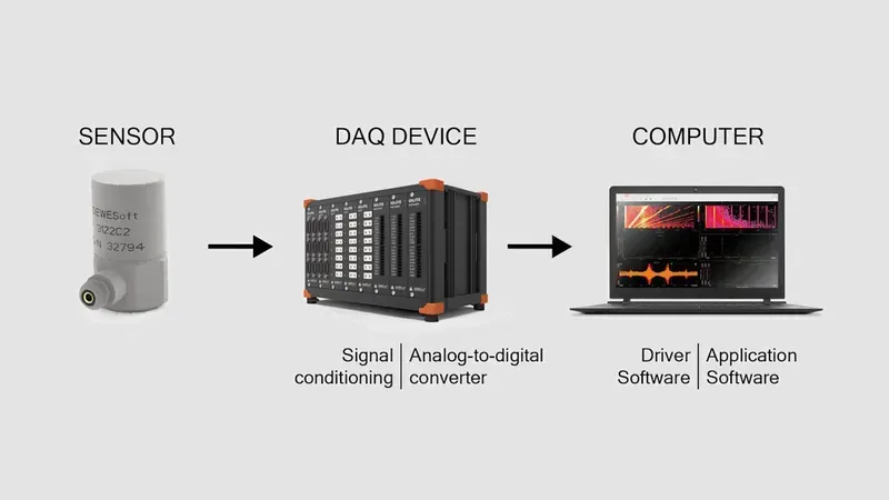
What are Data Acquisition Instruments? Data Acquisition (DAQ) instruments are electronic devices that measure physical phenomena, convert them into digital signals, and then transmit these signals for processing, analysis, and storage. They typically consist of sensors, signal conditioning circuitry, analog-to-digital converters (ADCs), and digital output interfaces.
Where are DAQ Instruments Primarily Applied? DAQ instruments are indispensable across a multitude of sectors, including industrial control and automation for process monitoring, scientific research for experimental data collection (e.g., aerospace, physics), medical diagnostics for physiological signal monitoring, automotive testing for performance analysis, and environmental monitoring for climate and pollution data.
Why is the PCB Crucial in DAQ Systems? The PCB is the foundational platform for all electronic components in a DAQ system, enabling precise signal routing, power distribution, and component integration. Its design directly influences signal integrity, noise susceptibility, thermal management, and overall system accuracy and reliability. A well-designed DAQ PCB ensures minimal signal degradation, accurate measurements, and robust performance in demanding environments.
How Does PCB Design Affect Signal Integrity in DAQ? In DAQ systems, signal integrity is paramount to avoid data corruption and measurement inaccuracies. PCB design elements such as trace impedance control, proper grounding schemes, minimal trace lengths, differential pair routing, and strategic component placement are crucial. These measures mitigate signal reflections, crosstalk, and electromagnetic interference (EMI), preserving the fidelity of sensitive analog signals during conversion and transmission.
What Role Does Performance Play in DAQ PCB Design? Performance in DAQ PCB design encompasses several factors: speed (data throughput), resolution (measurement precision), accuracy, and stability. High-performance DAQ PCBs utilize advanced materials with stable dielectric constants, implement sophisticated power integrity networks to ensure clean power for sensitive ADCs, and incorporate thermal management techniques to prevent performance drift due to temperature fluctuations, ultimately ensuring reliable and accurate data acquisition.
Key Considerations for DAQ PCB Design
Designing Printed Circuit Boards (PCBs) for Data Acquisition (DAQ) instruments demands meticulous attention to detail, as even minor imperfections can significantly compromise signal integrity and measurement accuracy. The core challenge lies in preserving the fidelity of sensitive analog and high-speed digital signals amidst potential interference, requiring a strategic approach to layout, power delivery, and thermal dissipation. Understanding these critical design factors is paramount to developing reliable and high-performance DAQ systems.
Signal Routing and Trace Layout Precise signal routing is fundamental to minimizing signal degradation in DAQ PCBs. Analog signals, particularly low-level ones, require isolation from noisy digital lines. This often involves employing separate signal layers, maintaining consistent trace impedances, and avoiding sharp bends to prevent reflections. Differential pairs for high-speed signals must be length-matched and tightly coupled to ensure common-mode noise rejection and consistent impedance. Careful consideration of via placement also prevents impedance discontinuities.
Noise Reduction Techniques Effective noise reduction is critical for accurate data acquisition. This encompasses robust grounding strategies, such as implementing a solid ground plane to provide a low-impedance return path for signals and shield against electromagnetic interference (EMI). Separation of analog and digital grounds, connected at a single point, can prevent digital noise from coupling into sensitive analog circuitry. Shielding, through guard rings or dedicated shielded traces, further protects sensitive signals from external interference and crosstalk, especially in mixed-signal designs.
Impedance Control Maintaining controlled impedance throughout the signal path is essential for high-speed DAQ systems. Mismatched impedances lead to signal reflections, which can distort waveforms and introduce errors, particularly in high-frequency data transmission. This requires precise control over trace width, dielectric thickness, and material properties. Specialized PCB manufacturing processes, like those offered by Zero One Solution Limited, are crucial to achieve and verify these tight impedance tolerances, ensuring signal integrity at higher data rates.
Thermal Management While often overlooked, effective thermal management is vital for the long-term reliability and performance of DAQ instruments. Components like ADCs, DACs, and FPGAs can generate significant heat, and elevated temperatures can lead to performance drift, reduced accuracy, and premature component failure. Design strategies include placing heat-generating components strategically, utilizing thermal vias to transfer heat to ground planes, incorporating sufficient copper pours for heat dissipation, and, in some cases, integrating heatsinks or active cooling solutions.
Material Selection for Optimal Performance
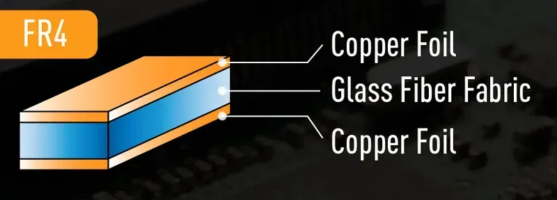
PCB Material FR-4
The selection of appropriate PCB materials is paramount in data acquisition (DAQ) instruments, directly influencing signal integrity, operational reliability, and overall system performance. Beyond the ubiquitous FR-4, specialized materials are often required to meet the stringent demands of high-frequency signals, precise analog measurements, and stable environmental operation, thereby ensuring optimal data fidelity.
Material Type
Dielectric Constant (Dk)
Dissipation Factor (Df)
Key Applications in DAQ
Advantages
Disadvantages
FR-4 (Standard)
4.2-4.7
0.015-0.020
General-purpose, lower frequency DAQ
Cost-effective, widely available
Higher signal loss at high frequencies, less stable Dk
High-Tg FR-4
~4.4
~0.015
High-temperature DAQ, power circuits
Improved thermal stability, enhanced reliability
Slightly higher cost than standard FR-4
Rogers (High-Frequency Laminates)
2.2-11.0
0.0009-0.004
High-speed data acquisition, RF/Microwave DAQ
Excellent signal integrity, low loss, stable Dk/Df
Higher cost, specialized manufacturing processes
Polyimide
~3.3-3.6
~0.005-0.010
Flexible DAQ systems, harsh environments
High temperature resistance, excellent flexibility
Higher cost than FR-4, less rigid
Beyond the fundamental electrical properties, material selection also considers mechanical stability, environmental resilience, and manufacturing compatibility. For instance, in applications demanding extreme temperature cycles or high humidity, materials with low moisture absorption and stable thermal expansion coefficients are crucial. Zero One Solution Limited leverages its deep understanding of these material characteristics to recommend and implement the most suitable PCB laminates, ensuring your DAQ instrument PCBs achieve peak performance and longevity.
High-Speed Signal Handling Techniques
High-Speed Signal PCB Trace
Mastering high-speed signal handling on Data Acquisition Instrument PCBs is paramount for ensuring data integrity and accuracy in modern DAQ systems, where even picosecond delays can lead to significant errors. This necessitates meticulous PCB design techniques that go beyond conventional practices, focusing on preserving signal quality across complex layouts.
Differential Signaling: The Noise Immunity Advantage Differential signaling involves transmitting a signal and its inverted copy on two separate traces. The receiver then processes the difference between these two signals, effectively canceling out common-mode noise induced by external electromagnetic interference (EMI) or power supply fluctuations. This technique is crucial for high-speed interfaces like LVDS (Low-Voltage Differential Signaling) and USB 3.0, ensuring robust data transmission in noisy environments common in industrial or scientific data acquisition. Implementing differential pairs requires precise trace routing, maintaining tight coupling and consistent impedance between the traces. According to industry standards, typical impedance for differential pairs is 100 ohms, although this can vary based on the specific interface.
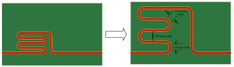
Trace Length Matching: Mitigating Skew and Timing Errors In high-speed digital designs, particularly with parallel interfaces or critical clock signals, precise trace length matching is essential. Unmatched trace lengths can lead to signal skew, where different bits or clock/data signals arrive at the receiver at different times, causing setup and hold time violations and ultimately data corruption. Modern EDA tools facilitate automated length matching, often employing serpentine routing (meandering traces) to equalize path lengths within acceptable tolerances. For DDR memory interfaces, for instance, trace length tolerances can be as tight as ±5 mils for speeds exceeding 800 Mbps, highlighting the precision required.
Technique
Primary Benefit
Key Design Consideration
Impact on DAQ Performance
Differential Signaling
Enhanced Noise Immunity
Precise Trace Coupling & Impedance
Improved Signal-to-Noise Ratio (SNR), Reliable Data Capture
Trace Length Matching
Eliminates Signal Skew
Precise Path Length Equalization
Accurate Timing, Reduced Bit Error Rate (BER)
Controlled Impedance
Minimizes Reflections
Consistent Trace Width & Dielectric
Clean Signal Transmission, Prevent Data Loss
Ground Plane Optimization
Reduces Noise & Crosstalk
Solid, Uninterrupted Ground Return Path
Stable Reference, Enhanced Signal Integrity
Decoupling Capacitance
Stable Power Delivery
Placement Near IC Pins
Reduced Power Supply Noise, Accurate Analog Measurements
Minimizing signal reflections is another critical aspect, achieved through meticulous impedance control. Reflections occur when a signal encounters an impedance mismatch along its path, bouncing back towards the source and causing signal degradation. This is mitigated by ensuring traces maintain a consistent characteristic impedance (e.g., 50 ohms for single-ended signals) matching the source and load impedances. Proper termination techniques, such as series or parallel resistors, are also employed at the end of transmission lines to absorb reflected energy. Moreover, careful consideration of stack-up design, including dielectric constant and layer spacing, is vital for achieving accurate impedance targets. Adhering to these high-speed techniques ensures the integrity of the collected data, which is paramount for the reliability and accuracy of any data acquisition instrument.
Power Integrity in Data Acquisition PCBs
PCB Decoupling Capacitor
Achieving stable and clean power delivery is paramount for the optimal performance and accuracy of data acquisition (DAQ) instruments. Any noise or fluctuation in the power supply can directly impact the sensitive analog-to-digital converters (ADCs), sensors, and signal conditioning circuitry, leading to inaccurate readings, reduced resolution, and overall system instability. Therefore, meticulous attention to power integrity (PI) during the PCB design phase is not merely a best practice but a fundamental requirement for reliable DAQ solutions.
Why is Power Integrity Crucial for DAQ Systems? Power integrity ensures a stable and low-noise voltage supply to all components, particularly sensitive analog and mixed-signal ICs. In DAQ systems, where precise measurement and minimal interference are critical, poor power integrity can introduce significant errors, manifesting as increased noise floor, reduced effective number of bits (ENOB) in ADCs, and compromised signal-to-noise ratio (SNR).
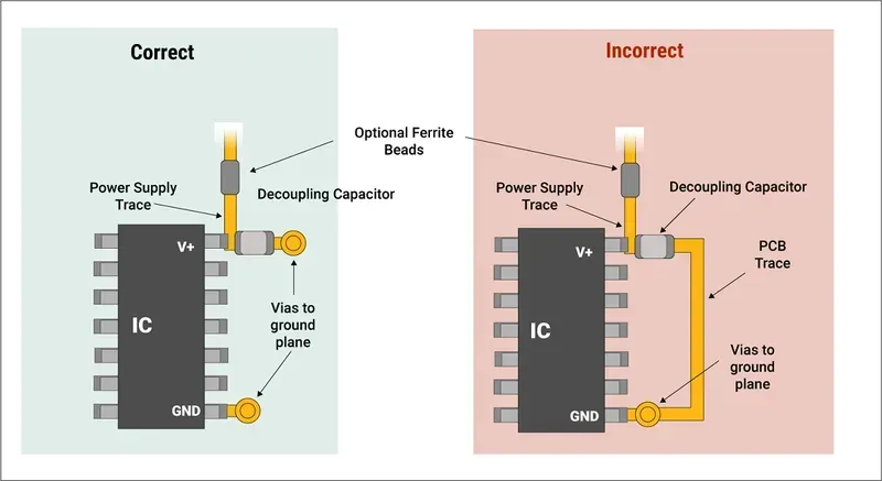
How do Decoupling Capacitors Enhance Power Integrity? Decoupling capacitors, placed strategically close to the power pins of integrated circuits, act as local charge reservoirs. They supply instantaneous current demands from switching logic and high-speed components, effectively shunting high-frequency noise from the power rails to the ground plane. This minimizes voltage droop (ground bounce and VCC sag) and prevents noise propagation across the board, critical for maintaining signal integrity in DAQ systems.
What are the Principles of Effective Power Plane Design? Effective power plane design involves creating low-impedance power and ground planes that provide a stable reference and efficient current return paths. This includes minimizing plane splits, ensuring sufficient plane overlap, and avoiding routing traces across high-current or sensitive areas. A well-designed power plane distributes current uniformly and minimizes inductive effects, crucial for reducing electromagnetic interference (EMI) and improving overall power delivery network (PDN) performance.
What is the Role of Impedance in Power Integrity? Low impedance in the power delivery network (PDN) is essential. A low impedance path from the voltage regulator module (VRM) to the component power pin ensures that voltage fluctuations are minimized during transient current demands. Designers target a target impedance profile across various frequencies, often employing a combination of bulk, mid-frequency, and high-frequency decoupling capacitors to maintain impedance below a critical threshold.
How does Zero One Solution Address Power Integrity in DAQ PCB Solutions? Zero One Solution Limited employs advanced simulation tools for power integrity analysis (e.g., PDN analysis) during the design phase. Our engineers meticulously plan power and ground plane distribution, optimize decoupling capacitor placement and value selection, and implement robust power regulation schemes. We prioritize multi-layer PCB stack-ups with dedicated power and ground planes to achieve ultra-low impedance and superior noise suppression, ensuring the highest signal integrity for your data acquisition instruments.
Manufacturing and Assembly Considerations
PCB Surface Finish
The manufacturing and assembly phases are critical for realizing the high-performance potential of a data acquisition (DAQ) instrument PCB design. Even the most meticulously engineered layout can be compromised by imprecise fabrication or improper component placement. Ensuring reliability and optimal signal integrity necessitates strict adherence to best practices in impedance control, selection of appropriate surface finishes, and accurate component placement, all of which directly impact the final system's accuracy and longevity.
Impedance Control Accurate impedance control is paramount for high-speed data acquisition, preventing signal reflections and ensuring clean data transmission. This involves precise control over trace width, dielectric constant of the material, and board stack-up. Manufacturers must utilize advanced fabrication techniques and employ time-domain reflectometry (TDR) testing to verify that trace impedances meet the specified tolerances, typically within ±10% for critical signals.
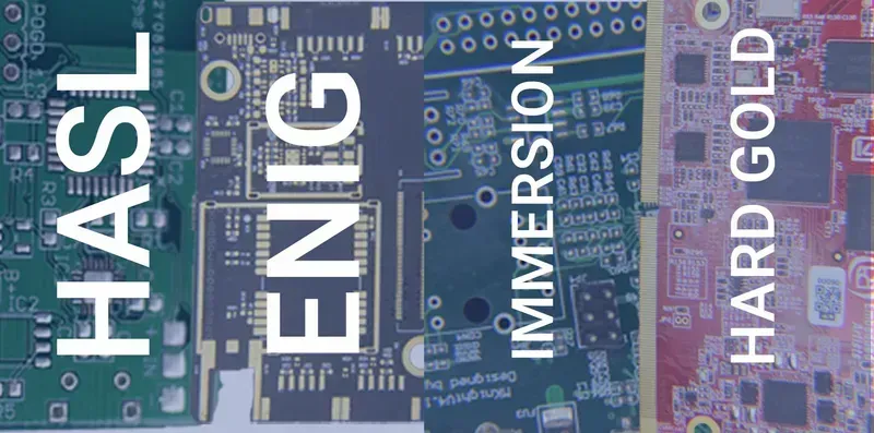
Surface Finish Selection The choice of surface finish significantly impacts solderability, shelf life, and signal integrity, particularly at high frequencies. Common finishes include Electroless Nickel Immersion Gold (ENIG), Immersion Silver (ImAg), and Organic Solderability Preservative (OSP). For DAQ PCBs, ENIG is often preferred due to its excellent flatness, which is crucial for fine-pitch components (e.g., ADCs, DACs) and wire bonding, along with its superior oxidation resistance. However, considerations like cost and high-frequency signal loss must be evaluated.
Component Placement Strategy Strategic component placement is essential for minimizing noise, optimizing signal paths, and managing thermal dissipation. Analog and digital sections should be isolated with separate ground planes or careful routing to prevent crosstalk. Sensitive components, like ADCs, should be placed away from noisy digital logic and power switching circuits. Additionally, thermal considerations dictate that heat-generating components are spaced adequately and aligned for efficient heat dissipation, potentially utilizing thermal vias or heatsinks.
Manufacturing Consideration
Impact on DAQ PCB Performance
Zero One Solution Limited's Approach
Trace Width Consistency
Directly affects impedance control, critical for high-speed signals.
Utilizes high-precision etching and advanced CAM software for tight tolerance control.
Drill Accuracy
Ensures proper via and pad registration, vital for signal path integrity.
Employs high-precision drilling machines with optical alignment systems.
Solder Paste Deposition
Influences solder joint quality and reliability, especially for fine-pitch components.
Uses advanced stencil printing with automated optical inspection (AOI) for precise volume control.
Reflow Soldering Profile
Determines component solderability and prevents thermal stress or damage.
Customizes thermal profiles for each board, considering component types and board complexity.
Assembly Cleanliness
Prevents contamination that can lead to electrical leakage or corrosion.
Maintains strictly controlled cleanroom environments and employs rigorous cleaning processes.
Zero One Solution Limited's Expertise in DAQ PCB Solutions
Zero One Solution Limited stands as a beacon of excellence in providing comprehensive PCB solutions for Data Acquisition (DAQ) Instruments. Our deep understanding of the intricate demands of DAQ systems, from maintaining signal integrity to ensuring robust power delivery, positions us as an ideal partner for developers seeking unparalleled performance and reliability. With over a decade of specialized experience since our inception in 2011, we streamline your product development lifecycle, offering a one-stop service from initial design consultation through to rapid prototyping, precise manufacturing, and efficient assembly, all while upholding the highest quality standards.
Rapid Prototyping for Accelerated Innovation We specialize in rapid-response R&D prototype manufacturing, enabling clients to quickly iterate and validate their DAQ instrument designs. Our agile processes drastically reduce time-to-market, allowing for faster product launches and competitive advantage in the rapidly evolving electronics landscape.
End-to-End Design to Assembly Services Our integrated approach covers every stage of the PCB journey for DAQ instruments. From meticulous layout design, ensuring optimal signal paths and noise reduction, to precision manufacturing and sophisticated assembly, we guarantee consistency and quality across the entire production chain. This holistic service minimizes complexities and maximizes efficiency for our clients.
Service Aspect
Zero One Solution Limited's Advantage
Benefit for DAQ Instrument Development
PCB Design Optimization
Expertise in high-speed signal routing, impedance control, and noise reduction specifically for DAQ.
Ensures superior signal integrity and measurement accuracy for sensitive DAQ applications.
Material Sourcing & Selection
Access to a global network of high-performance PCB materials (e.g., Rogers, Isola) suitable for high-frequency DAQ.
Guarantees optimal electrical properties and thermal stability under diverse operating conditions, enhancing instrument longevity.
Precision Manufacturing
Advanced fabrication capabilities including fine-line etching, multilayer registration, and stringent quality control.
Delivers PCBs with tight tolerances crucial for complex DAQ circuitry and high-density component integration.
Leveraging our strategic locations in Shenzhen and Dubai, we tap into a robust global PCBA supply chain, ensuring access to the latest technologies and resources. Our commitment to quality is unwavering, with rigorous testing and inspection protocols implemented at every stage. Partner with Zero One Solution Limited to transform your innovative DAQ instrument concepts into high-performing, market-ready products with exceptional speed and precision.
Case Studies: Successful DAQ PCB Projects
Data Acquisition PCB Project
At Zero One Solution Limited, our commitment to excellence in Data Acquisition (DAQ) Instrument PCB solutions is best demonstrated through our successful project implementations. We consistently tackle complex challenges, delivering high-performance, reliable PCBs that meet the stringent demands of modern DAQ systems. These case studies highlight our technical prowess and our ability to translate intricate requirements into tangible, functional hardware.
Project Focus
Key Challenges
Zero One Solution's Approach
Achieved Outcomes
High-Precision Scientific DAQ
Achieving sub-microvolt noise levels and extreme temperature stability for sensitive analog front-ends.
Utilized advanced low-DF substrates (e.g., Rogers 4003C), implemented multi-layer stack-ups with dedicated ground planes, and optimized component placement for minimal crosstalk.
Delivered PCBs with <0.5µV noise floor, enabling precise data capture in critical scientific experiments. Exceeded client's thermal stability requirements (±0.01% drift over -40°C to +85°C).
Multi-Channel Industrial DAQ for Harsh Environments
Ensuring signal integrity and robust operation in high-EMI industrial settings with high channel count (100+ channels).
Employed extensive shielding layers, controlled impedance routing for all digital and analog lines, and selected durable, chemically resistant solder masks. Implemented robust power delivery networks with advanced decoupling.
Successfully deployed over 1000 units with zero field failures due to PCB issues. Achieved stable data acquisition performance even under significant electromagnetic interference, enhancing factory floor reliability.
These examples underscore our holistic approach, from material selection and intricate design considerations to precision manufacturing and assembly, ensuring that every DAQ PCB we produce functions optimally within its intended application environment. Our rapid prototyping capabilities also played a crucial role, allowing for quick design iterations and accelerated time-to-market for our clients.
FAQs about Data Acquisition PCB Design and Manufacturing
Navigating the complexities of Data Acquisition (DAQ) PCB design and manufacturing often leads to common inquiries regarding signal integrity, material choices, and production best practices. A deep understanding of these FAQs is crucial for ensuring the reliability and high performance of DAQ instruments, which are at the core of accurate data collection in various industries.
What are the primary challenges in designing PCBs for high-precision data acquisition? The primary challenges in high-precision DAQ PCB design revolve around maintaining signal integrity, minimizing noise, and ensuring stable power delivery. This includes meticulous layout for sensitive analog signals, effective grounding and shielding strategies, precise impedance control, and thermal management to prevent drift and maintain accuracy. The goal is to isolate sensitive analog paths from noisy digital logic and power domains.
How does material selection impact the performance of a DAQ PCB? Material selection profoundly impacts DAQ PCB performance by influencing signal loss, impedance stability, and thermal characteristics. For high-speed or high-frequency DAQ, materials with lower dielectric constant (Dk) and dissipation factor (Df) like certain Rogers laminates are preferred over standard FR-4 due to their reduced signal attenuation and better impedance control. Thermal stability of the material also affects long-term reliability and measurement accuracy in varying environments.
What signal integrity considerations are most critical for data acquisition PCBs? Critical signal integrity considerations for DAQ PCBs include minimizing reflections, crosstalk, and electromagnetic interference (EMI). This is achieved through controlled impedance routing, careful trace length matching for differential pairs, proper termination, and robust grounding schemes (e.g., solid ground planes). Effective power integrity (PI) is also crucial, ensuring stable and noise-free power rails for sensitive ADCs and other analog components through appropriate decoupling and power plane design.
Why is precise impedance control essential in DAQ PCB manufacturing? Precise impedance control is essential in DAQ PCB manufacturing to ensure predictable signal propagation and minimize reflections, especially for high-speed digital and analog signals. Deviations from target impedance can lead to signal degradation, increased bit error rates, and inaccurate analog measurements. Manufacturers achieve this through careful control of trace width, dielectric thickness, and material properties during fabrication, often verifying with TDR (Time Domain Reflectometry) testing.
In conclusion, a well-designed and manufactured PCB is the backbone of any high-performance data acquisition instrument. Zero One Solution Limited is committed to providing comprehensive PCB solutions that meet the demanding requirements of data acquisition applications. From initial design and rapid prototyping to manufacturing and assembly, we empower our clients to develop cutting-edge DAQ systems with confidence. Contact us today to discuss your data acquisition PCB needs and let us help you turn your innovative ideas into reality. Share your thoughts and experiences with data acquisition PCB solutions in the comments below!