In today's tech-driven world, smart projectors are revolutionizing entertainment and presentations. At the heart of these sophisticated devices lies the Printed Circuit Board (PCB), a critical component that dictates performance, reliability, and overall functionality. Zero One Solution Limited offers cutting-edge PCB solutions specifically tailored for smart projectors, ensuring optimal performance and seamless integration. With our headquarters in Shenzhen, the heart of China's electronics manufacturing, and a branch in Dubai, we stand at the center of a global PCBA supply chain, ready to support your innovations.
Introduction to Smart Projector PCBs
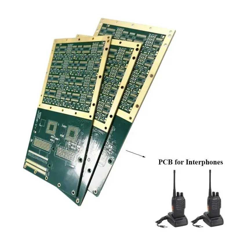
Smart projector PCB board
At the core of every smart projector lies a sophisticated Printed Circuit Board (PCB), serving as the central nervous system that orchestrates all electronic functions. These specialized PCBs are critical for integrating advanced features such as high-resolution video processing, wireless connectivity, smart operating systems, and interactive capabilities. Without a meticulously designed and manufactured PCB, the seamless performance, vibrant image quality, and intelligent functionalities that define a modern smart projector simply wouldn't be possible. Therefore, understanding the pivotal role of these PCBs is paramount for anyone involved in the development, manufacturing, or even procurement of smart projection technology.
Why are Smart Projector PCBs fundamentally different from standard PCBs? Smart projector PCBs differ significantly from conventional PCBs due to their specialized requirements for high-speed data processing, advanced thermal management, and compact integration of diverse functionalities. They must handle high-bandwidth video signals (e.g., 4K/8K), support multiple wireless protocols (Wi-Fi, Bluetooth), and manage the heat generated by powerful projection light sources and processors, all within a constrained form factor. This necessitates multi-layer designs, precise impedance control, and often the use of specialized, heat-dissipating materials, which are not typically found in general-purpose PCBs.
What are the primary functions a PCB performs within a smart projector? The PCB in a smart projector performs a multitude of critical functions, including: video processing and scaling to manage various input resolutions and output to the display engine; power management for efficient energy distribution to all components, especially the high-power light source and CPU/GPU; data transmission for internal communication and external connectivity; audio processing for integrated sound systems; and control logic for user interface, sensor integration, and overall system operation. It essentially acts as the backbone for all computational, communication, and power delivery tasks.
How does PCB design influence the performance and longevity of a smart projector? PCB design profoundly impacts a smart projector's performance and longevity. Signal integrity, crucial for high-resolution video and high-speed data transfer, prevents artifacts and ensures crisp images. Effective thermal management through optimized copper pour, via placement, and material selection prevents component overheating, extending the lifespan of critical components like LEDs/lasers and processors. Furthermore, robust power delivery networks minimize voltage drops and noise, ensuring stable operation. Poor design in any of these areas can lead to degraded image quality, system instability, and premature hardware failure.
What specific challenges are faced when designing PCBs for compact smart projectors? Designing PCBs for compact smart projectors presents unique challenges primarily due to space constraints and thermal density. Miniaturization demands higher component density, leading to increased heat generation in a smaller volume, making thermal management significantly more complex. Signal integrity also becomes more challenging with shorter trace lengths and potential for crosstalk. Additionally, integrating diverse functionalities (processing, wireless, power) into a confined multi-layer structure while ensuring manufacturability and cost-effectiveness requires advanced design techniques and sophisticated simulation tools.
Key Considerations in Smart Projector PCB Design
Designing Printed Circuit Boards (PCBs) for smart projectors presents unique challenges that demand meticulous attention to detail. The core objective is to create a robust and efficient platform that supports high-performance optical engines, complex processing units, and integrated connectivity while maintaining optimal thermal conditions. Key considerations include thermal management to dissipate heat generated by high-power LEDs and processors, ensuring signal integrity for reliable data transmission, and strategic component selection to meet performance, size, and cost targets. These intertwined factors are critical for the longevity, stability, and overall user experience of a smart projector.
Thermal Management Strategies Effective thermal management is paramount in smart projector PCB design due to the significant heat generated by high-power LEDs, CPUs, and GPUs. Strategies include utilizing multi-layer PCBs with optimized copper pour for heat spreading, incorporating thermal vias, and selecting substrates with high thermal conductivity (e.g., CEM-3, FR-4 with enhanced thermal properties). Additionally, integrating heatsinks and considering active cooling solutions (fans) in the overall system design are crucial to prevent thermal throttling and extend component lifespan. Simulation tools, such as CFD (Computational Fluid Dynamics), are often employed to predict thermal behavior and optimize heat dissipation paths.
Ensuring Signal Integrity and Power Integrity With high-speed data transmission required for video processing and network connectivity, maintaining signal integrity (SI) is vital. This involves careful impedance matching, controlled trace geometries, proper termination techniques, and minimizing crosstalk through differential pair routing and strategic component placement. Power integrity (PI) is equally important to ensure stable voltage delivery to sensitive components, requiring robust power planes, appropriate decoupling capacitor placement, and minimizing ground bounce. Both SI and PI are critical for preventing data corruption, reducing electromagnetic interference (EMI), and ensuring stable system operation, especially in compact, high-density designs.
Strategic Component Selection Component selection profoundly impacts the performance, cost, and manufacturability of smart projector PCBs. This involves choosing high-efficiency power management ICs, low-noise amplifiers for audio circuits, compact and high-performance processors for image rendering, and reliable wireless modules for connectivity (Wi-Fi, Bluetooth). Factors like package size, power consumption, operating temperature range, and long-term availability are critical. Opting for automotive-grade or industrial-grade components might be necessary for extended operational lifespans and resilience in varying environments, balancing performance requirements with cost-effectiveness and supply chain stability.
Minimizing Electromagnetic Interference (EMI) Smart projectors are susceptible to and can generate significant EMI due to their high-speed digital circuits and switching power supplies. Effective EMI suppression techniques are essential for compliance with regulatory standards and preventing interference with other electronic devices. This includes careful grounding schemes, shielding, proper trace routing to minimize loop areas, filtering power lines, and selecting components with low EMI signatures. Designing for EMC (Electromagnetic Compatibility) from the outset reduces costly rework and ensures a reliable product that operates seamlessly in diverse environments.
Compactness and Miniaturization The increasing demand for portable and sleek smart projectors necessitates highly compact PCB designs. This often leads to multi-layer boards, use of smaller package components (e.g., BGA, QFN), and high-density interconnect (HDI) technologies. While miniaturization saves space, it introduces challenges related to thermal management, trace routing complexity, and manufacturability. Designers must balance the need for compactness with considerations for heat dissipation, ease of assembly, and testability, often requiring advanced design software and close collaboration with manufacturing partners like Zero One Solution Limited to achieve optimal results.
Zero One Solution's Expertise in Projector PCBs
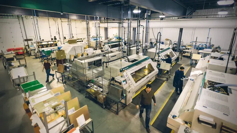
PCB manufacturing factory
Zero One Solution Limited stands at the forefront of PCB innovation, particularly in the demanding realm of smart projector technology. Our extensive experience, honed over years in Silicon Valley and Shenzhen, positions us as a trusted partner for designing and manufacturing high-quality, high-performance Smart Projector PCBs that are critical for achieving superior image processing, thermal management, and compact integration in advanced projection systems.
How does Zero One Solution ensure optimal thermal management in Smart Projector PCBs? We employ advanced thermal simulation software and design techniques, incorporating specialized PCB materials with high thermal conductivity (e.g., aluminum-based or copper-invar-copper laminates), strategic component placement, and integrated heat dissipation solutions such as thermal vias and robust copper planes to effectively manage heat generated by high-power components like LED/laser drivers and display processors, preventing performance degradation and extending product lifespan.
What signal integrity challenges does Zero One Solution address in Smart Projector PCB design? Smart projectors transmit high-speed video and data signals. We mitigate signal integrity issues through controlled impedance routing, meticulous stack-up design, differential pair routing for high-speed interfaces (HDMI, DisplayPort), careful via management, and comprehensive signal integrity analysis, ensuring clear, stable video output and reliable data transfer.
What types of advanced PCB materials does Zero One Solution utilize for Smart Projector PCBs? Beyond standard FR-4, we leverage a range of specialized materials tailored for projector demands, including high-Tg laminates for thermal stability, low-loss materials for high-frequency signal integrity, and metal-core PCBs (MCPCBs) or thick copper layers for superior thermal dissipation from powerful light sources and processing units.
How does Zero One Solution support rapid prototyping for Smart Projector PCB development? Our rapid prototyping capabilities, a core strength, enable quick iteration and validation of Smart Projector PCB designs. We offer expedited fabrication and assembly services, leveraging our advanced manufacturing facilities and streamlined processes to deliver functional prototypes in significantly reduced lead times, accelerating product development cycles for our clients.
What quality control measures are in place for Zero One Solution's Smart Projector PCB manufacturing? Our commitment to quality is upheld through stringent quality control protocols at every stage. This includes Automated Optical Inspection (AOI), X-ray inspection for hidden solder joints (BGAs), In-Circuit Testing (ICT), Functional Testing (FCT), and environmental stress screening to ensure the reliability, performance, and longevity of every Smart Projector PCB before shipment.
PCB Materials and Technologies for Enhanced Performance
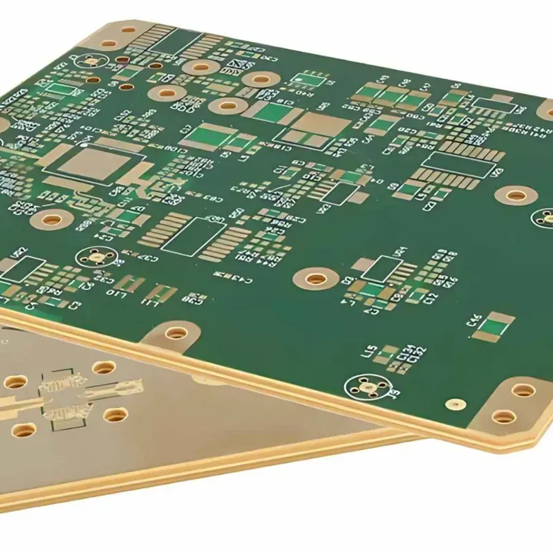
High performance PCB material
The foundation of a high-performance smart projector lies not only in its innovative design but critically, in the advanced PCB materials and cutting-edge technologies employed. These choices directly impact signal integrity, thermal dissipation, power efficiency, and overall product longevity, transforming a concept into a robust, market-ready device. Selecting the right materials and integrating state-of-the-art technologies is paramount for ensuring the projector’s optical and processing capabilities operate at their peak, delivering the immersive visual experiences users demand.
Advanced PCB Materials The selection of PCB substrate materials is crucial for managing high-frequency signals and heat. For smart projectors, which often integrate complex wireless modules (Wi-Fi, Bluetooth) and powerful projection engines, materials with low dielectric constant (Dk) and low dissipation factor (Df) are preferred. Examples include FR-4 variants with enhanced thermal properties, high-Tg (glass transition temperature) laminates, and for more demanding applications, ceramic-filled hydrocarbon materials like those from Rogers Corporation. These materials minimize signal loss and distortion, ensuring stable data transmission and reducing thermal stress on components.
High-Density Interconnect (HDI) Technology HDI PCBs are essential for compact smart projectors, allowing for denser component placement and finer traces. This technology utilizes microvias (laser-drilled holes) and sequential build-up layers, enabling more complex circuitry in a smaller footprint. Benefits include improved electrical performance due to shorter signal paths, enhanced reliability, and reduced electromagnetic interference (EMI). HDI is critical for integrating multiple functionalities, such as advanced image processing units, memory, and connectivity modules, within the constrained space of a projector.
Thermal Management Solutions Heat generated by projection light sources (LEDs/Lasers) and high-performance processors is a significant challenge. Advanced PCB designs incorporate integrated thermal solutions. This includes employing thicker copper layers for better heat spreading, using thermal vias to transfer heat to heat sinks, and incorporating metal core PCBs (MCPCBs) or ceramic substrates, especially for LED driver circuits. Efficient thermal management prevents component degradation, ensures consistent performance, and extends the lifespan of the smart projector. Zero One Solution Limited rigorously applies thermal simulation tools to optimize heat dissipation strategies in every design.
Embedded Component Technology Embedding passive and active components directly within the PCB layers offers multiple advantages for smart projectors. This technology reduces board size, improves electrical performance by shortening interconnections, enhances EMI shielding, and increases design flexibility. For example, embedding capacitors or resistors can free up surface real estate for more critical components like microprocessors or optical interfaces, leading to more compact and powerful projector designs.
Rapid Prototyping for Smart Projector PCBs
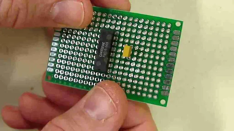
PCB rapid prototype sample
In the fast-evolving landscape of smart projector technology, rapid prototyping of PCBs is not merely an advantage but a critical necessity for accelerating product development and ensuring design accuracy. It enables engineers to quickly validate designs, identify potential flaws, and iterate on improvements, significantly reducing time-to-market and mitigating costly rework in later stages. This agile approach is fundamental to staying competitive and delivering innovative smart projector solutions that meet demanding performance and reliability benchmarks.
Why is rapid prototyping crucial for smart projector PCB development? Rapid prototyping is crucial because it allows for quick iteration and validation of design concepts. For smart projectors, which integrate complex optical, thermal, and electronic systems, early detection of issues related to signal integrity, thermal dissipation, or component placement can save significant time and resources. It supports a fail-fast approach, enabling engineers to refine designs based on real-world performance data rather than theoretical models, thereby accelerating the entire product development cycle from concept to market readiness. This agility is vital in a competitive market where time-to-market directly correlates with market share and innovation leadership.
Manufacturing and Assembly Processes
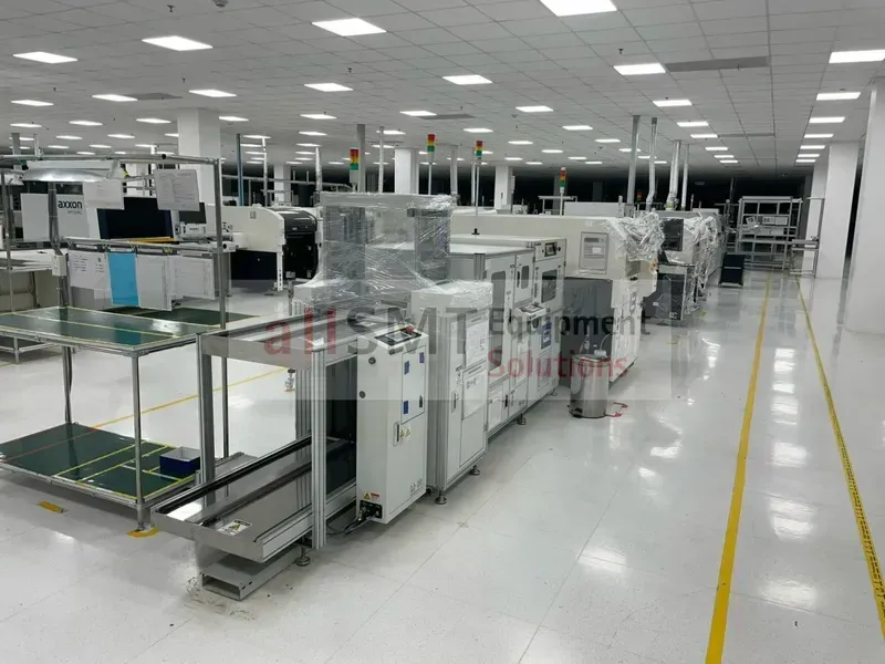
SMT production line
Zero One Solution Limited employs state-of-the-art manufacturing and assembly processes crucial for producing high-reliability smart projector PCBs, ensuring every board meets the demanding performance and longevity requirements of advanced projection systems. Our integrated approach covers every stage, from precise bare board fabrication to complex surface mount technology (SMT) and robust final assembly, all optimized for efficiency and unparalleled quality.
Automated SMT Line Precision Our manufacturing facilities leverage fully automated Surface Mount Technology (SMT) lines. This includes high-speed pick-and-place machines capable of accurately mounting ultra-fine pitch components and micro BGAs, essential for the compact and densely packed circuitry found in smart projector PCBs. Advanced solder paste inspection (SPI) and automated optical inspection (AOI) systems are integrated inline to detect and rectify defects at early stages, ensuring component placement accuracy and solder joint integrity, which are critical for high-frequency signal transmission in display applications. This minimizes manual errors and significantly enhances throughput and reliability, meeting strict IPC standards for electronic assemblies. Our lines are capable of handling a wide array of component types, including passive components down to 01005 size and complex IC packages, ensuring flexibility for diverse projector designs. The controlled environment within our SMT lines, including temperature and humidity, further safeguards component and material integrity during the assembly process. This level of automation is paramount for producing the consistent quality required for high-volume projector manufacturing, where even microscopic imperfections can impact optical and digital performance. The precise control over reflow profiles, often tailored to specific solder paste chemistries and component thermal sensitivities, is maintained to prevent thermal stress on sensitive components like display drivers and video processors. This ensures optimal solder joint formation, preventing issues such as voiding and insufficient wetting, which could lead to intermittent failures in the field.
Process Stage
Key Technology/Equipment
Benefit for Smart Projector PCBs
Bare Board Fabrication
Advanced CNC Drilling, Multi-layer Lamination Presses, Laser Direct Imaging (LDI)
Creates precise vias and complex multi-layer structures for high-speed signal integrity and dense component placement, vital for compact projector designs. Achieves tighter tolerances for enhanced performance and miniaturization.
Rigorous Quality Assurance at Every Step Beyond initial inspections, Zero One Solution implements comprehensive quality gates throughout the manufacturing and assembly process. This includes X-ray inspection for hidden solder joints (e.g., under BGAs), functional testing tailored to the specific operational parameters of smart projectors, and environmental stress screening (ESS) to identify potential failures under various conditions. Our quality management system is ISO 9001 certified, ensuring adherence to the highest international standards. Each PCB undergoes thorough visual inspections, electrical testing (e.g., flying probe, in-circuit test), and often burn-in tests to simulate real-world usage scenarios. This multi-layered approach to quality control significantly reduces the likelihood of defects reaching the final product, bolstering the reputation and reliability of the projectors our PCBs power. This commitment to quality is paramount for products like smart projectors, where reliability directly impacts user experience and brand perception. For smart projector PCBs, this means verifying the integrity of high-speed data lines, power delivery networks for LEDs/lasers, and control circuits for image processing, ensuring stable and consistent performance under continuous operation.
Process Stage
Key Technology/Equipment
Benefit for Smart Projector PCBs
Component Sourcing & Incoming Inspection
Global Supply Chain Network, Automated Component Verification Systems (e.g., LCR meters, XRF)
Ensures authenticity and quality of critical components (e.g., display drivers, image processors, power management ICs) to prevent performance degradation and ensure long-term reliability. Reduces supply chain risks and ensures component compliance with specifications.
Optimized Final Assembly and Integration Our final assembly stage incorporates precise manual and semi-automated processes for components that cannot be machine-placed, such as connectors, heatsinks, and specialized shielding. This includes skilled technicians performing selective soldering and conformal coating application to protect sensitive circuitry from environmental factors like dust and humidity, common in various usage environments for projectors. We also manage the integration of various sub-assemblies, ensuring seamless functionality. The entire process is meticulously documented and traceable, providing complete transparency from raw material to finished PCB. This detailed tracking system enables rapid problem-solving and continuous improvement, critical for meeting the evolving demands of the smart projector market. Our expertise extends to integrating complex optical and thermal management components directly onto the PCB, ensuring optimal alignment and performance, which is vital for the light engine and display modules of smart projectors. This holistic approach to manufacturing and assembly guarantees that each PCB delivered by Zero One Solution Limited is not just a component, but a reliable foundation for high-performance smart projector systems. The meticulous handling of sensitive optical and thermal elements during this stage is crucial to prevent damage or misalignment that could impact the projector's visual output and longevity.
Quality Control and Testing
Ensuring the unwavering reliability and optimal performance of smart projector PCBs is paramount, and at Zero One Solution Limited, this is achieved through a meticulously rigorous quality control and testing framework. Our commitment to excellence is deeply embedded in every stage of the PCB lifecycle, from initial design verification to final functional testing, guaranteeing that each board meets the highest industry standards and client specifications.
How does Zero One Solution ensure the quality of smart projector PCBs? Zero One Solution implements a multi-faceted quality assurance program that begins with stringent material selection and continues through design verification, in-process inspections, and comprehensive post-manufacturing testing. Our quality management system adheres to international standards, employing advanced inspection technologies and experienced personnel to identify and rectify any potential defects proactively. This holistic approach ensures consistent quality and reliability for every smart projector PCB.
What testing procedures are typically applied to smart projector PCBs? Typical testing procedures for smart projector PCBs include Automated Optical Inspection (AOI) for visual defects, In-Circuit Testing (ICT) to verify component placement and solder integrity, Flying Probe Testing for complex boards with high density, and functional testing to simulate real-world operating conditions and ensure the PCB meets all performance specifications. Environmental testing, such as thermal cycling and humidity tests, may also be performed for specific applications to validate long-term durability.
Why is rigorous quality control important for smart projector PCBs? Rigorous quality control for smart projector PCBs is crucial because these components are the core of the projector's functionality. Any defect can lead to image distortion, system failure, or reduced lifespan, directly impacting user experience and brand reputation. High-quality PCBs ensure stable performance, accurate image projection, efficient power management, and ultimately, a reliable and durable smart projector, minimizing warranty claims and maximizing customer satisfaction.
Zero One Solution Limited's expertise in Smart Projector PCB Solutions is best exemplified through our successful collaborations, where we've translated complex requirements into high-performance, reliable products. These case studies highlight our commitment to innovation, rapid prototyping, and stringent quality control, demonstrating how our tailored PCB solutions drive market-leading smart projectors.
Client
Project Scope
Challenges Addressed
Zero One Solution's Contribution
Outcome
Leading Consumer Electronics Brand
Compact 4K Smart Projector
Thermal management in a small form factor, high-speed data integrity
Developed a multi-layer PCB with advanced thermal dissipation techniques and optimized signal routing.
Achieved stable 4K projection in a highly compact design, enabling market differentiation and rapid product launch.
.
Portable Smart Projector with Battery Power
Power efficiency, miniaturization, robust connectivity for IoT features
Designed a low-power consumption PCB with integrated wireless modules and optimized component placement.
Delivered a highly portable projector with extended battery life and seamless smart home integration, exceeding performance targets.
.
High-Lumen Industrial Smart Projector
High current handling, long-term reliability in demanding environments, efficient power delivery
Engineered a heavy-copper PCB with enhanced power planes and robust component selection for industrial-grade durability.
Ensured stable operation and extended lifespan for a high-lumen projector used in continuous commercial applications, reducing maintenance costs.
The Future of Smart Projector PCB Technology
The trajectory of smart projector PCB technology is continuously evolving, driven by the insatiable demand for enhanced performance, miniaturization, and advanced functionalities. Future developments will focus on integrating higher levels of intelligence and connectivity directly onto the PCB, pushing the boundaries of what these compact devices can achieve. This evolution is critical for smart projectors to remain at the forefront of immersive visual experiences, seamlessly blending computing power with display technology.
What are the key emerging trends in Smart Projector PCB technology? Emerging trends include the adoption of advanced flexible and rigid-flex PCBs for greater design freedom and space optimization, the integration of System-on-Package (SiP) and heterogeneous integration for higher component density and reduced form factors, and the increased use of High-Density Interconnect (HDI) and Any-Layer HDI (ALHDI) technologies for superior signal integrity and miniaturization. Furthermore, advancements in thermal management materials and embedded cooling solutions are becoming critical to handle the increasing power density of integrated components.
How will AI and Machine Learning influence future Smart Projector PCB designs? AI and Machine Learning (ML) will profoundly impact PCB designs by enabling more sophisticated on-device processing. This will necessitate PCBs capable of handling higher data throughput and complex computational loads, likely leading to specialized AI accelerators, optimized memory architectures, and enhanced power delivery networks directly on the board. Furthermore, AI-driven design tools will likely automate and optimize complex routing and component placement, reducing development cycles and improving performance.
Combines multiple ICs and passive components into a single package, reducing board space and interconnects.
Ultra-miniaturization, improved electrical performance, enhanced reliability, lower power consumption.
What role will sustainable materials play in the future of Smart Projector PCBs? Sustainability is becoming an increasingly important factor. Future Smart Projector PCBs will likely incorporate more eco-friendly materials, such as halogen-free laminates, biodegradable substrates, and lead-free solders. Research into recyclable and renewably sourced materials for PCB manufacturing will also gain traction, aiming to reduce the environmental footprint of electronic waste and align with global sustainability initiatives.
Future Technology
Impact on Smart Projector PCBs
Benefits
High-Density Interconnect (HDI) and Any-Layer HDI
Allows for higher circuit density, finer lines and spaces, and smaller vias.
Increased functionality within a smaller footprint, improved signal integrity, enhanced thermal performance due to denser packing.
How will thermal management in Smart Projector PCBs evolve? As component density and processing power increase, thermal management will evolve to include integrated cooling solutions. This could involve embedding heat pipes or vapor chambers directly within the PCB layers, utilizing advanced thermal interface materials, and designing boards with optimized copper distribution for heat dissipation. Active cooling mechanisms, like micro-fans or thermoelectric coolers, might also become more common for ultra-compact, high-performance smart projectors.
Future Technology
Impact on Smart Projector PCBs
Benefits
Embedded Components
Passive and active components are embedded within the PCB layers.
Further miniaturization, reduced parasitic effects, improved signal integrity, enhanced reliability.
What are the challenges for manufacturers in adapting to these future PCB technologies? Manufacturers will face challenges in developing new fabrication processes for advanced materials, investing in high-precision equipment for finer feature sizes and heterogeneous integration, and adapting quality control measures for complex SiP and embedded technologies. The need for highly skilled labor in design, manufacturing, and testing will also be paramount to successfully implement these next-generation Smart Projector PCB solutions.
In conclusion, Zero One Solution Limited provides comprehensive and reliable PCB solutions for smart projectors, ensuring high performance and rapid prototyping. Our expertise in PCB design, manufacturing, and assembly, combined with our strategic global presence, positions us as the ideal partner for your smart projector development needs. Contact us today to discover how our tailored PCB solutions can bring your innovative projector designs to life. Elevate your visual experience – choose Zero One Solution.