In today's fast-paced electronics industry, understanding the cost of PCB fabrication is crucial. JLCPCB, a leading PCB manufacturer, offers a streamlined online quoting process. This guide delves into the intricacies of a JLCPCB quote, ensuring you grasp all the essential elements for cost-effective PCB production, just like choosing the right components for a powerful circuit.
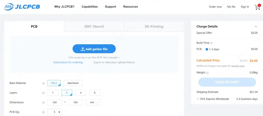
The JLCPCB online quote system provides an efficient method for obtaining pricing for your PCB fabrication needs. This section details a step-by-step approach for utilizing their quote calculator, ensuring accurate cost estimations and a smooth transition to production. A thorough understanding of this process is crucial for cost-effective PCB manufacturing.
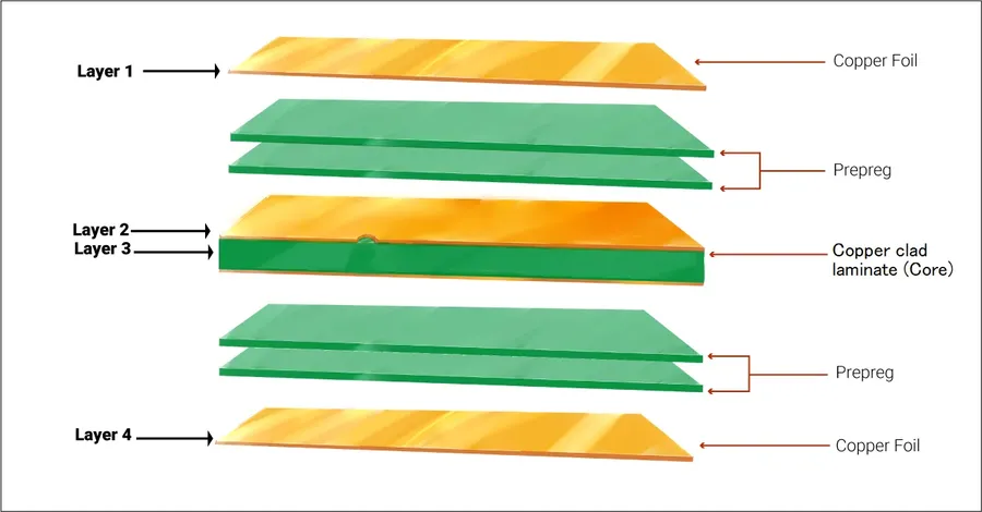
The cost of your printed circuit board (PCB) from JLCPCB is significantly influenced by the materials you select and the number of conductive layers your design requires. These two factors are fundamental in determining the base price before considering other features and options. Understanding these influences is critical for cost-effective PCB design and procurement.
| Material Type | Description | Cost Impact | Typical Applications |
|---|---|---|---|
| FR-4 | Most common PCB material, a glass-reinforced epoxy laminate. Offers a good balance of performance and cost. | Base cost, lowest of commonly used materials. | Most standard PCBs, general purpose use. |
| Aluminum | A metal core PCB that provides excellent heat dissipation. Aluminum core is laminated between two copper layers. | Higher cost than FR-4, due to material and fabrication process. | LED lighting, power electronics, high-heat applications. |
| Rogers | High-performance materials designed for high-frequency applications with low signal loss. | Significantly higher cost than FR-4 due to specialized material and manufacturing. | RF and microwave circuits, high-speed digital applications. |
| CEM-1/CEM-3 | Paper or composite material, More affordable than FR-4 with some reduced performance. | Lower cost, suitable for cost-sensitive applications. | Consumer electronics, low-end applications. |
The number of layers is also critical, each layer adds to the complexity and material requirements. Layer count significantly impacts cost and must be considered as a core element of design
| Layer Count | Description | Cost Impact | Design Complexity |
|---|---|---|---|
| Single Layer | Simplest PCB design with conductive traces on one side of the board. | Lowest cost option. | Simple circuits, basic electronics. |
| Double Layer | Conductive traces on both sides of the board. | Slightly higher cost than single layer. | Most intermediate designs. |
| 4 Layer | Two signal layers, a power plane, and a ground plane. Provides better signal integrity. | Moderate increase in cost, commonly used for more complex digital circuits. | Complex circuits, high density designs |
| 6+ Layer | Multiple signal and power/ground planes. Required for highly complex and dense circuits. | Highest cost, necessary for complex digital circuits, high layer count may be required for impedance control. | High density interconnect, complex signal routings. |
For example, opting for standard FR-4 material and fewer layers is a cost-effective decision for simpler designs, while high-speed applications will require Rogers material with multiple layers. Always balance your performance needs with cost considerations.
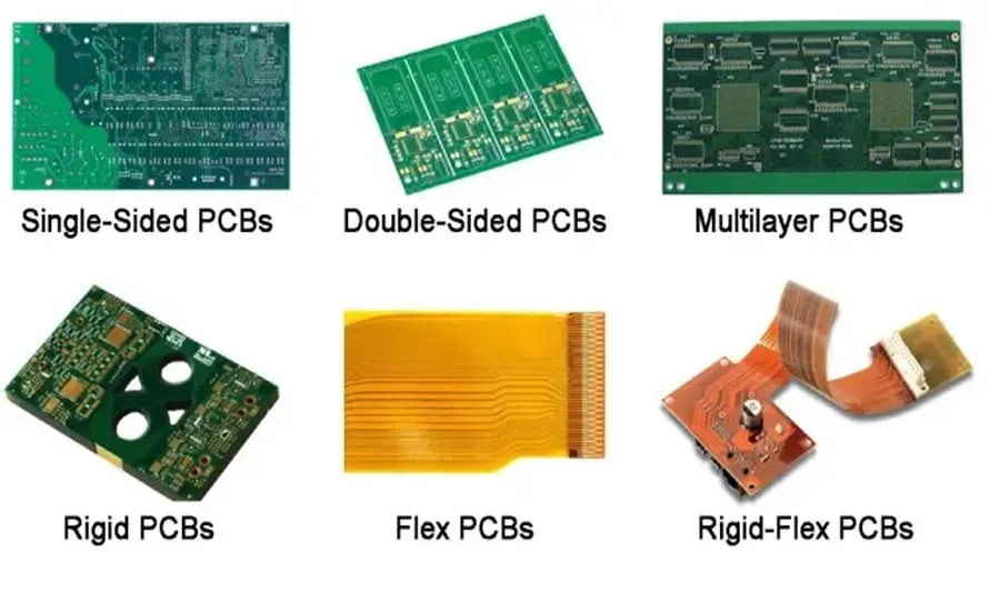
The physical dimensions of your printed circuit board (PCB) and the quantity you order are primary drivers of the overall fabrication cost at JLCPCB. Understanding how these factors interact can lead to significant savings. Larger boards generally require more material and processing time, thus increasing cost. Similarly, the economies of scale heavily influence pricing, with larger production runs significantly lowering the unit cost.
The price of a PCB is not simply a linear relationship with its size; there are often breakpoints where the price increases. Similarly, the cost per board decreases dramatically as the order quantity increases, which makes strategic purchasing a crucial aspect of PCB manufacturing. This chapter provides actionable strategies to optimize cost through careful planning and a good understanding of JLCPCB's pricing model.
| Factor | Description | Impact on Cost |
|---|---|---|
| PCB Size | The physical dimensions of the PCB (length and width). | Larger boards generally cost more due to increased material usage and processing time. |
| Order Quantity | The number of PCBs ordered in a single batch. | Larger quantities result in lower per-unit costs due to economies of scale. |
| Panelization | Combining multiple PCB designs into a single manufacturing panel. | Reduces cost per board by optimizing material utilization and handling during manufacturing. |
Panelization is a key technique to lower costs, which involves grouping multiple individual boards into one larger panel for production. By doing this, you effectively use more of the manufacturing resources in one setup and share setup costs across more individual boards. JLCPCB offers a panelization service and also accepts panelized designs directly, but it’s important to design your panel correctly so that the boards can be easily separated afterwards. In some cases, the panelization itself can add to the cost due to the increased complexity of handling the larger panel.
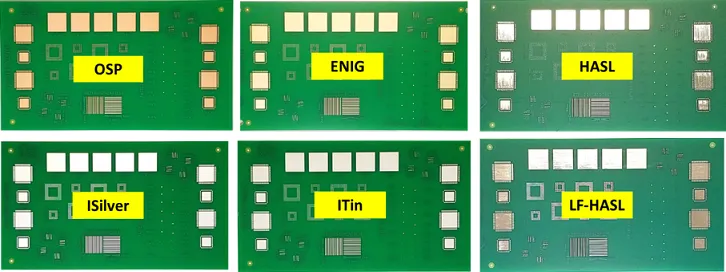
The surface finish of a Printed Circuit Board (PCB) is a critical factor influencing its performance, reliability, and ultimately, cost. Different finishes offer varying levels of solderability, oxidation resistance, and electrical conductivity, making the selection process a trade-off between functionality and budget. This section provides a detailed analysis of common surface finish options offered by JLCPCB and their associated pricing implications, which are core to getting an accurate JLCPCB quote.
| Surface Finish | Description | Pros | Cons | Cost Implications |
|---|---|---|---|---|
| HASL (Hot Air Solder Leveling) | A process where molten solder is applied to the PCB and then leveled with hot air. | Low cost, good solderability, readily available. | Uneven surface finish, not suitable for fine-pitch components, contains lead (lead-based HASL). | Generally the most affordable option. |
| Lead-Free HASL | Similar to HASL but uses a lead-free solder alloy. | Good solderability, RoHS compliant, relatively low cost. | Less even surface than ENIG, may not be ideal for very fine pitch components. | Slightly more expensive than standard HASL but still considered a lower cost option. |
| ENIG (Electroless Nickel Immersion Gold) | A two-layer metallic finish, nickel provides a barrier layer and gold acts as the solderable and corrosion resistant surface. | Excellent solderability, flat surface, good for fine-pitch components, long shelf life, good corrosion resistance. | More expensive than HASL. | Higher cost, primarily due to the use of gold, but provides superior performance in many applications. |
| OSP (Organic Solderability Preservative) | A thin organic coating that protects copper pads from oxidation. | Flat surface, good solderability, lead-free, relatively low cost. | Shorter shelf life, sensitive to handling, may require a more stringent assembly process. | Lower cost compared to ENIG, but may introduce some handling and assembly considerations. |
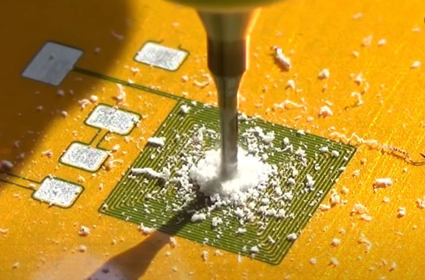
The precision and quantity of drilled holes significantly influence the cost of PCB fabrication. This section delves into how drill size specifications, the number of holes, and the choice between standard vias and microvias affect your JLCPCB quote, guiding you towards an optimal balance of functionality and cost.
| Specification | Impact on Cost | Design Consideration |
|---|---|---|
| Number of Holes | Directly Proportional: More holes generally increase cost due to increased drilling time and tool wear. | Minimize unnecessary vias and consider design alternatives. |
| Drill Size (Diameter) | Smaller drill sizes, particularly below 0.3mm, often increase cost. Microvias significantly more costly. | Use standard sizes whenever possible and avoid overly small holes if not needed. |
| Standard Vias | Typically less expensive than microvias, suitable for most layer transitions. | Use for most through-hole and layer-to-layer connections. |
| Microvias | More expensive due to specialized drilling and plating processes. Facilitates denser designs. | Use when board space is critically constrained and fine-pitch routing is required. |
Optimizing hole specifications involves a careful consideration of both functionality and cost implications. Where possible, adhere to JLCPCB's standard drill sizes and minimum hole specifications to avoid unnecessary cost inflation. Additionally, using standard vias where appropriate reduces cost compared to microvias while still ensuring reliable electrical connections.
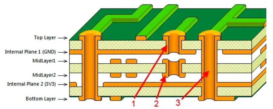
Advanced PCB features, while enhancing performance and functionality, significantly influence fabrication costs. These features often require specialized processes and tighter tolerances, resulting in increased expenses. Understanding the cost implications of these features is critical for optimizing your PCB design and budget.
| Feature | Description | Cost Impact | Design Considerations |
|---|---|---|---|
| Impedance Control | Ensures controlled signal impedance for high-speed circuits. Requires precise trace dimensions and dielectric properties. | High | Requires careful stack-up planning and trace width calculations. |
| Gold Fingers | Gold-plated edge connectors for enhanced durability and conductivity. Commonly used for card edge connections. | Medium to High | Requires precise gold plating thickness specifications. |
| 45° Finger Chamfering | Angled edges on gold fingers that facilitate smoother insertion and reduce wear on the mating connector. | Medium | Needs extra fabrication process and precise cutting. |
| Blind and Buried Vias | Vias that connect specific layers, not passing through the entire board. Enables higher density routing. | Medium to High | Requires extra drilling and plating steps. |
| Via-in-Pad (VIP) | Placing vias directly within the surface mount pads. It increases routing density and space. | Medium | Requires filled or plated over vias, may need special attention. |
Understanding shipping costs and lead times is crucial when ordering PCBs from JLCPCB. These factors significantly impact your project timeline and budget, particularly when transitioning from prototypes to mass production. Careful planning can mitigate unexpected expenses and delays, ensuring a smooth manufacturing process.
| Shipping Option | Typical Lead Time (Days) | Cost (USD) | Notes |
|---|---|---|---|
| Standard Shipping | 7-15 | Variable, based on weight and destination | Most economical option for non-urgent orders. |
| Expedited Shipping (e.g., DHL, FedEx) | 3-7 | Higher than standard, varies by carrier | Suitable for time-sensitive projects. |
| Air Freight (for large quantities) | 5-10 | Cost-effective for bulk orders | Requires coordination and custom clearance processes. |
The lead time provided by JLCPCB typically includes manufacturing and assembly time, while the shipping lead time depends on the courier and destination. It's crucial to consider both when estimating the total turnaround time for your project. Factors such as order complexity, component availability, and any necessary rework will influence these times. Lead times should always be validated with JLCPCB's current lead-time projections, as they can fluctuate depending on workload.
Several factors influence the final shipping cost, including the weight and dimensions of the package, the shipping destination, and the selected carrier. JLCPCB's online platform will generate the shipping quote after you've completed the project details and selected the desired shipping option. In general, planning ahead and opting for consolidated shipments whenever possible can significantly reduce these costs, especially when transitioning from small prototypes to larger mass production.
Understanding your JLCPCB quote is crucial for efficient and cost-effective PCB manufacturing. This section addresses frequently asked questions to clarify common concerns and provide clear answers.
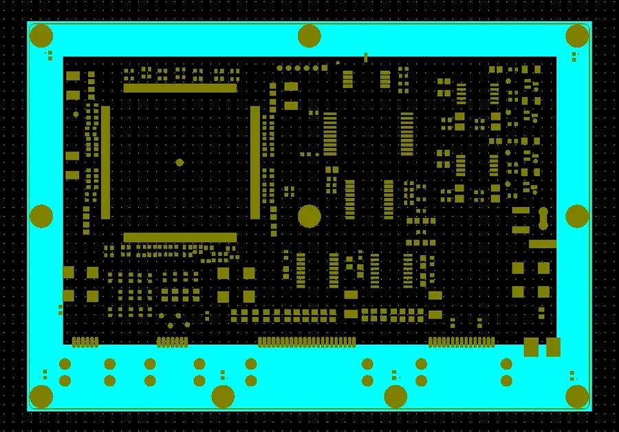
Optimizing your PCB design and order parameters is crucial for minimizing fabrication costs at JLCPCB. By employing smart design strategies and adhering to standard specifications, you can significantly reduce your overall expenditure without compromising on quality. This section provides actionable strategies to achieve the best possible JLCPCB quote.
Understanding the intricacies of a JLCPCB quote empowers you to make informed decisions, optimizing both cost and quality for your PCB projects. Just like a well-designed circuit that integrates various components, a well-understood quote ensures a successful project. Leveraging JLCPCB’s platform and this guide, you’re set to streamline your fabrication process and bring your electronics designs to life. [jlcpcb quote]

