
In the rapidly evolving landscape of Advanced Driver Assistance Systems (ADAS), the demand for high-resolution, ultra-compact camera modules is at an all-time high. However, packaging complex high-speed electronics into limited footprints introduces significant engineering challenges. This guide provides the definitive DFM playbook for achieving reliable, high-yield manufacturing for rigid-flex circuits.
Understanding the Rigid-Flex Advantage in Camera Modules
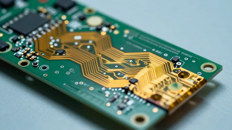
In the evolution of automotive imaging, the transition from rigid boards with discrete cabling to integrated rigid-flex assemblies represents a fundamental shift in reliability and miniaturization. Rigid-flex circuits eliminate mechanical connectors—the primary failure point in high-vibration automotive environments—while allowing for complex three-dimensional routing within the confined housing of a camera module.
Comparative Analysis: Traditional vs. Rigid-Flex Assemblies
| Feature | Traditional Rigid with Cables | Rigid-Flex Integration |
|---|---|---|
| Mechanical Reliability | Low (Connector fatigue risk) | High (Solder-joint integrity) |
| Spatial Footprint | High (Bulkier volume) | Minimal (Dynamic bending) |
| Signal Integrity | Variable (Cabling interference) | Optimal (Controlled impedance) |
| Assembly Speed | Manual intensive | Automated/Reduced parts |
Key Advantages for High-Speed Interconnects
Modern rearview cameras rely on high-speed data protocols like GMSL or FPD-Link. Rigid-flex designs provide superior signal integrity by maintaining consistent trace geometry through the transition zones between the image sensor board and the main processing unit. By reducing impedance mismatches inherent in connectors, these circuits support higher data rates with lower electromagnetic interference (EMI).
Frequently Asked Questions
- Why is rigid-flex preferred over traditional ribbon cables?
Ribbon cables introduce connectors that are susceptible to fretting corrosion and vibrational disconnects; rigid-flex replaces these with permanent, flexible polyimide circuits that handle thermal cycling significantly better. - Does rigid-flex impact manufacturing DFM requirements?
Yes, it necessitates stricter control over bend radii and localized reinforcement of transition zones to prevent delamination during the assembly process. - How does rigid-flex aid in thermal management?
The integrated nature of the flex material allows for more efficient heat dissipation paths compared to discrete wire harnesses, which can block airflow and act as insulators.
Strategic Stack-Up Configuration for High-Speed Signal Integrity

Engineering Balanced Stack-ups for High-Speed Performance
For miniaturized rearview camera modules, the PCB stack-up is the primary defense against crosstalk and signal degradation. A symmetric stack-up design—where signal layers are mirrored across the center core—is essential to prevent board warpage during the high-temperature reflow process common in automotive manufacturing. By utilizing a balanced construction, engineers can maintain consistent dielectric spacing, which is critical for achieving tight impedance tolerances required by MIPI CSI-2 and other high-speed serial interfaces.
Substrate Selection and Material Properties
The choice of dielectric material impacts both signal loss (Df) and thermal management. Standard FR-4 is often insufficient for high-frequency camera data; instead, low-loss, high-glass transition temperature (Tg) materials are mandated to ensure long-term reliability under the harsh thermal cycling conditions of vehicle exteriors.
| Material Property | High-Speed Requirement | Design Rationale |
|---|---|---|
| Dielectric Constant (Dk) | Low and Stable | Maintains precise impedance control. |
| Dissipation Factor (Df) | Very Low (<0.005) | Reduces signal attenuation at high frequencies. |
| Tg (Glass Transition) | >170°C | Ensures structural integrity during thermal shock. |
Best Practices for Impedance Control
- How do you minimize impedance discontinuities at interconnects?
Avoid stitching via stubs and ensure ground reference planes are continuous beneath high-speed differential pairs; use back-drilling if necessary to remove excess copper in the barrel. - What is the role of reference plane stitching?
Stitching vias should be placed periodically along the return path to maintain a low-inductance loop, preventing EMI emissions from the high-speed data bus. - Why prioritize trace width accuracy in DFM?
In miniaturized boards, manufacturing tolerances for trace width (etching factor) can significantly shift impedance; specify +/- 10% tolerance to your fabricator early in the design cycle.
/* Example Stack-up Constraint for High-Speed Layers */
layer_1: Signal (Microstrip, 100 ohm diff)
layer_2: Ground (Reference)
layer_3: Signal (Stripline, 90 ohm diff)
layer_4: Ground (Reference)
Mastering Trace Width and Spacing Rules
Managing Fine-Pitch Trace Geometries
In high-density rearview camera modules, the conflict between routing density and fabrication limits is acute. To maintain signal integrity, designers must strictly adhere to the manufacturer's capabilities regarding copper thickness, etching tolerances, and dielectric spacing. As traces shrink toward 3-mil or below, the aspect ratio of the trace becomes the primary factor in determining the feasibility of the design.
| Parameter | Standard Yield (High-Volume) | Advanced HDI Requirement |
|---|---|---|
| Minimum Trace Width | 4.0 mil | 2.0 - 2.5 mil |
| Minimum Trace Spacing | 4.0 mil | 2.0 - 2.5 mil |
| Copper Weight | 0.5 oz (standard) | 0.25 - 0.33 oz (thin) |
High-Speed Interconnect Considerations
High-speed differential pairs for MIPI CSI-2 interfaces are sensitive to manufacturing variances. Variations in trace width along the interconnect length introduce impedance discontinuities, causing return loss at the receiver. To mitigate this, prioritize trace symmetry and use controlled-depth drilling for blind and buried vias to minimize parasitic inductance.
Best Practices for DFM Efficiency
- How do copper thickness requirements affect trace etching?
Thicker copper requires wider spacing to prevent shorting during the chemical etching process. For ultra-fine pitch designs, utilize thinner starting copper foil to achieve narrower, more precise trace profiles. - What is the impact of trace shape on signal integrity?
Avoid trapezoidal trace cross-sections caused by over-etching. Consistent rectangular profiles are essential for maintaining stable impedance across high-frequency camera data links. - When should teardropping be implemented?
Always apply teardropping at pad-to-trace junctions. This reinforces mechanical strength and prevents trace cracking during thermal cycling in harsh automotive environments.
Via-in-Pad Technology: Balancing Density and Reliability
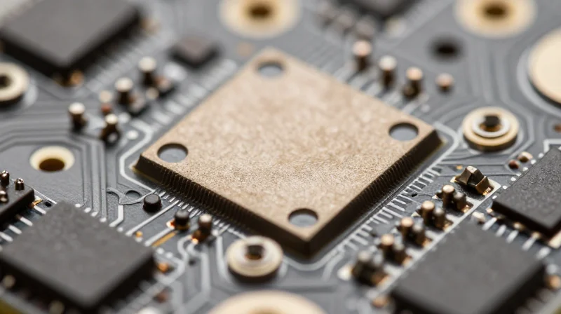
Via-in-Pad Technology: Balancing Density and Reliability
Via-in-pad (VIP) is the cornerstone of miniaturized automotive design, allowing components to be placed directly over vias to save precious board real estate. By eliminating the 'dog-bone' fan-out pattern, designers can significantly shorten trace lengths, which is critical for reducing signal degradation in high-speed LVDS or MIPI CSI-2 interfaces found in rearview cameras. However, the proximity of the solder joint to the via structure introduces risks such as solder wicking and voiding, which must be mitigated through robust manufacturing processes.
Critical DFM Considerations for Via-in-Pad
| Parameter | Recommendation | Reasoning |
|---|---|---|
| Plating Thickness | Minimum 20-25µm | Ensures structural integrity during thermal expansion. |
| Capping Process | Copper-filled & Over-plated | Prevents solder wicking and provides a planar surface. |
| Via Diameter | Typically < 0.15mm | Balances drilling precision with plating access. |
Preventing Common Fabrication Defects
The primary danger in VIP designs is the entrapment of manufacturing fluids or air within the via barrel, which can lead to 'outgassing' during reflow. This phenomenon creates voids that compromise both electrical connectivity and mechanical strength. To achieve automotive-grade reliability, it is mandatory to use a Copper Capped (VIPPO) process. This involves filling the via with conductive or non-conductive epoxy, followed by electrolytic copper plating to flatten the surface. This creates a solid pad identical to a surface mount land, preventing solder from draining into the via during assembly.
- Why is copper filling preferred over non-conductive epoxy for rearview camera PCBs?
Copper filling provides superior thermal conductivity and a Coefficient of Thermal Expansion (CTE) matched to the surrounding board, reducing stress on the via barrel during the extreme temperature fluctuations experienced in automotive environments. - How can I inspect for internal via-in-pad voids?
Standard AOI is insufficient; cross-sectional analysis and X-ray inspection are required post-reflow to verify the absence of solder voids and ensure the copper cap remains flush with the pad surface. - Does via-in-pad increase manufacturing costs?
Yes, it adds steps for filling, leveling, and over-plating. However, this is offset by the reduced board size and improved signal integrity, which are higher priorities for miniaturized camera modules.
Flexibility and Bending Radius Constraints
Optimizing Bending Radius for Long-Term Reliability
For miniaturized automotive camera systems, the bending radius is the primary determinant of flex-circuit longevity. To prevent delamination, copper fatigue, and trace cracking, designers must adhere to a minimum bending radius defined as a multiple of the total circuit thickness. For standard polyimide-based flex, a general rule of thumb is to maintain a radius at least 10 to 15 times the thickness of the flexible section for dynamic applications, or 6 to 10 times for static, installation-only bends.
| Bend Type | Recommended Ratio (R/T) | Application Note |
|---|---|---|
| Static (Installation) | 6x - 10x | One-time bend for chassis fitment |
| Dynamic (Repetitive) | 15x - 20x | High-vibration automotive environments |
| Stiffener Interface | 10x | Maintain distance from rigid transitions |
Mechanical Design Best Practices
To ensure durability under harsh automotive thermal cycling and vibration, the transition from rigid to flexible zones must be carefully managed. Implementing 'I-beam' construction avoidance by staggering traces on opposite sides of the flex layer prevents excessive stress concentration during bending. Furthermore, ensuring that the neutral axis is aligned with the center of the conductive layers minimizes internal strain on copper signals.
- How does trace routing affect bend durability?
Traces should be routed perpendicularly to the bend line whenever possible and utilize curved, rather than sharp-angled, trace transitions to distribute mechanical stress evenly. - Why should teardrops be used on flex pads?
Teardropping pads prevents trace 'necking' and provides a larger contact area, which significantly reduces the likelihood of pad lifting during mechanical movement or thermal expansion. - What role do stiffeners play in flex design?
Stiffeners provide mechanical support at connector interfaces and component mounting areas, but must be tapered to prevent a sudden change in stiffness that could cause cracking at the transition boundary.
Minimizing Manufacturing Risks with DFM Simulation

The Role of Virtual Prototyping in Miniaturized Electronics
In the context of miniaturized automotive rearview cameras, physical prototyping is prohibitively expensive and time-consuming. Modern DFM simulation bridges this gap by creating a virtual replica of the manufacturing process, allowing engineers to stress-test high-speed interconnects and dense routing layouts under simulated thermal and mechanical conditions before a single board is etched.
Critical DFM Validation Metrics
| Risk Factor | Simulation Focus | Production Impact |
|---|---|---|
| Solder Bridging | Fine-pitch mask clearance analysis | Prevents electrical shorts on high-density ICs |
| Acid Traps | Geometry-based trace-angle checking | Avoids etching irregularities in high-speed traces |
| Via Reliability | Plating thickness uniformity | Ensures connectivity in high-vibration automotive environments |
Integrating EDA Tools for Early Error Detection
Effective DFM is not a final check but a continuous loop. By embedding DFM validation directly into the EDA workflow, designers receive real-time feedback on manufacturing violations. This proactive approach is particularly crucial when dealing with high-speed serial links, where trace length matching and impedance control are highly sensitive to even minor manufacturing deviations.
- How does DFM software reduce automotive recall risks?
By identifying potential fatigue points in flex-rigid joints and via structures, simulation ensures that components can withstand the rigorous thermal cycling and vibration profiles defined by automotive standards. - Why is automated DFM preferred over manual design rule checks?
Automated simulation accounts for physical fabrication tolerances (like chemical etching rates and material flow), which manual rule sets often overlook, providing a more accurate prediction of final yield.
Optimizing Assembly Processes for Miniaturized PCBs
Precision Solder Mask and Surface Finish Selection
For high-density interconnect (HDI) rearview camera boards, solder mask registration is critical. To prevent solder bridging and minimize misregistration errors, specify Liquid Photoimageable (LPI) solder masks with high registration tolerances. Regarding surface finishes, the choice directly impacts assembly reliability.
| Finish Type | Best For | Assembly Limitation |
|---|---|---|
| ENEPIG | Fine-pitch BGA/Wire bonding | Costlier than alternative finishes |
| ENIG | Reliable solder joints | Susceptible to 'black pad' syndrome |
| Immersion Silver | High-speed signals | Environmentally sensitive to sulfur |
Automated Assembly Considerations
Miniaturized components, such as 01005 passives and micro-BGAs, demand advanced assembly capabilities. To achieve consistent yield, designers must work closely with manufacturing partners to ensure the stencil design accommodates the high aspect ratio of the apertures, preventing solder starvation on fine-pitch pads.
- Why is stencil thickness critical for miniaturized PCBs?
Thin stencils (typically 0.05mm to 0.1mm) are essential to maintain the correct area ratio for tiny apertures, ensuring clean paste release and preventing solder shorts. - How do you mitigate component skew during reflow?
Ensure symmetrical thermal relief designs in copper pours and implement optimized reflow profiles with extended soak times to allow for uniform thermal distribution across high-density zones. - Are fiducial requirements different for micro-assemblies?
Yes, high-precision global and local fiducials are mandatory, typically requiring a minimum of three marks per board to allow the pick-and-place machines to compensate for panel-level distortions.
Scaling for Mass Production in Automotive Markets
Transitioning from Prototype to Mass Production
Moving from initial design iterations to full-scale production necessitates a rigorous focus on Design for Manufacturing (DFM) to mitigate failure rates. In automotive applications, the shift involves ensuring that tolerances are sufficiently loose for mass-production machinery while remaining tight enough for high-speed signal integrity. Engineers must standardize components to minimize the Bill of Materials (BOM) complexity, thereby reducing procurement risk and improving throughput in Surface Mount Technology (SMT) assembly lines.
Production Strategy Comparison
| Parameter | Prototype Focus | Mass Production Focus |
|---|---|---|
| Component Selection | Performance-centric | Reliability and Availability-centric |
| Panel Utilization | Low (Cost secondary) | High (Optimized array density) |
| Tolerance Control | Precision-manual | Statistical Process Control (SPC) |
| Testing Method | Functional Bench testing | Automated Optical & In-Circuit Testing |
Critical DFM Strategies for Automotive Scaling
- How does PCB panelization impact manufacturing costs?
Optimizing board layout within the fabrication panel minimizes material waste and increases throughput, which is essential for achieving target unit costs in high-volume automotive runs. - Why is component standardization vital?
Standardizing footprints and parts reduces the risk of supply chain bottlenecks and allows for higher speed automated pick-and-place operation without frequent machine adjustments. - How can one guarantee automotive reliability at scale?
Implement strict Design for Testing (DFT) protocols, including integrated test points for In-Circuit Testing (ICT), ensuring every board undergoes verification for signal speed and thermal integrity before deployment. - What role does traceability play in mass production?
Automotive standards require robust traceability; incorporate unique serial identification via laser marking on every PCB to track assembly variables and material batches throughout the product lifecycle.
To achieve high-yield production, designers must collaborate closely with Contract Manufacturers (CMs) early in the design phase. By validating the PCB design against the specific capabilities of the assembly equipment, you avoid late-stage redesigns and costly manufacturing delays. Focus on optimizing the solder stencil design and thermal profiles for reflow ovens, ensuring that the high-speed interconnects remain stable across thousands of repeated cycles.
Successfully designing rigid-flex PCBs for ADAS camera modules requires a perfect balance between electrical performance and mechanical durability. By adhering to these DFM best practices, your team can reduce prototype iterations and ensure seamless transitions to mass manufacturing. Contact our engineering team today to review your current design files and optimize your path to production.
