
In the fast-evolving automotive electronics sector, the push for smarter, safer vehicles is straining traditional manufacturing margins. As rearview vision systems become standard, suppliers face a critical challenge: delivering high-performance components while minimizing physical footprints. This article explores how transitioning to advanced, miniaturized PCB designs serves as the linchpin for both cost-efficiency and technical excellence.
The Shift Toward Miniaturization in Modern Automotive Systems
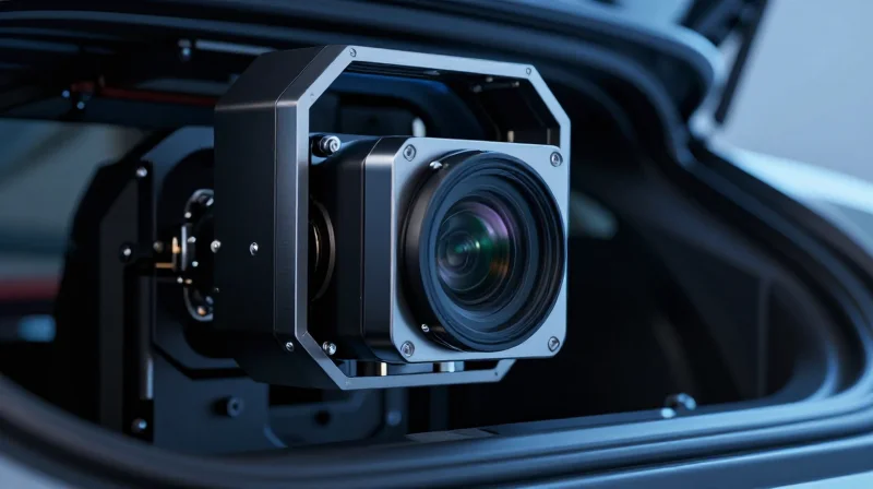
The Drivers of Automotive Miniaturization
The mandate for smaller camera modules in modern vehicles is not merely an aesthetic preference but a functional necessity. As advanced driver-assistance systems (ADAS) move toward higher levels of autonomy, the sheer volume of camera sensors required per vehicle has surged. This density forces engineers to reclaim space within side mirrors, bumpers, and roof lines, necessitating highly optimized, miniaturized PCB designs that do not compromise signal integrity or thermal performance.
Strategic Impact on ROI
Miniaturization directly influences ROI by reducing the physical material footprint of the hardware and improving the packaging efficiency of the final assembly. By consolidating functions and reducing board dimensions, manufacturers can lower per-unit material costs and decrease vehicle curb weight, which is essential for extending the range of electric vehicles.
| Design Constraint | Miniaturization Strategy | ROI Benefit |
|---|---|---|
| Spatial Volume | High-Density Interconnect (HDI) PCBs | Increased sensor integration density |
| System Weight | Advanced substrate materials | Reduced fuel/battery consumption |
| Thermal Management | Integrated heat dissipation layers | Extended component operational lifespan |
Frequently Asked Questions
- Why is board space becoming such a critical bottleneck?
Modern vehicles must house multiple cameras for surround-view, blind-spot monitoring, and LIDAR-fusion systems, all competing for limited real estate within the chassis. - Does smaller PCB size always equate to higher production costs?
While advanced HDI processes require initial capital investment, the long-term ROI is achieved through higher yields, reduced material usage, and enhanced scalability across multiple vehicle platforms. - How does miniaturization affect signal integrity?
Miniaturization requires sophisticated electromagnetic interference (EMI) shielding and high-speed routing strategies to ensure data transmission remains stable despite the physical proximity of components.
Material Waste Reduction: The Economic and Environmental Case
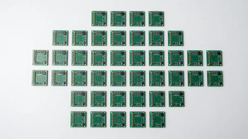
In the hyper-competitive automotive electronics sector, the economic viability of camera module production hinges on material efficiency. As PCB footprints shrink to accommodate compact housing, the strategy of maximizing panel utilization—placing more circuit boards onto a standard manufacturing panel—becomes a primary driver for reducing scrap rates and lowering unit costs. By refining design rules to permit tighter spacing without compromising signal integrity, manufacturers can drastically reduce the amount of wasted substrate material, directly translating into improved margins and a lower carbon footprint.
The Economic Impact of Panel Utilization
| Optimization Strategy | Economic Benefit | Environmental Impact |
|---|---|---|
| Increased Array Density | Higher throughput per panel | Lower per-unit substrate consumption |
| Reduced Keep-out Zones | Lower material scrap per board | Reduced chemical waste in etching |
| Panel Size Standardization | Optimized logistics and supply chain | Decreased packaging and transport emissions |
Key Questions on Design Efficiency
- How does miniaturization directly lower production overhead?
Smaller footprints allow for a higher count of PCBs per manufacturing panel. This increased density reduces the number of panels processed for the same target volume, thereby lowering machine-hour costs and raw material consumption. - Can tighter spacing lead to manufacturing risks?
While tighter spacing maximizes material usage, it requires advanced fabrication capabilities. Utilizing high-density interconnect (HDI) technologies helps maintain yields while minimizing the physical gap between circuits, offsetting the risks of manufacturing defects. - Why is material waste a sustainability concern in camera module production?
Traditional sub-optimal layouts often lead to excessive 'frame' and 'bridge' waste. By optimizing the board geometry to fit closer, companies minimize the extraction and disposal impact of pre-preg, copper foil, and hazardous etching chemicals.
Ultimately, the transition toward advanced miniaturization is not merely a spatial necessity for modern ADAS architectures; it is a financial imperative. By viewing PCB layout as a material-optimization problem rather than just a circuit-design problem, engineers can unlock hidden value, turning raw material conservation into a sustainable competitive advantage in the automotive supply chain.
Streamlining Assembly Time for Automotive Suppliers
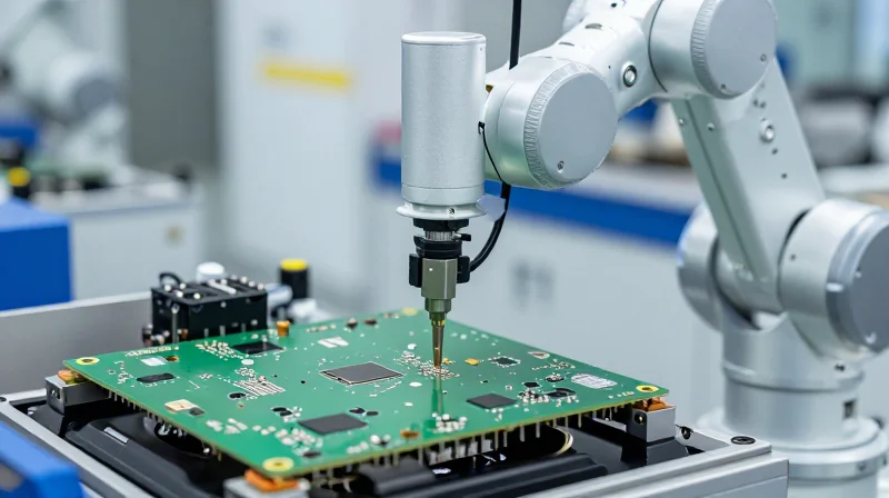
Streamlining Assembly Time for Automotive Suppliers
For automotive suppliers, the bottleneck in camera module production often lies in the Surface Mount Technology (SMT) assembly line. By transitioning to standardized, high-density miniaturized PCB designs, manufacturers can achieve tighter component placement tolerances and faster pick-and-place speeds. This approach minimizes nozzle travel time, reduces the frequency of feeder swaps, and facilitates a more streamlined automated optical inspection (AOI) process.
Design Strategies for Throughput Optimization
- Uniform Component Orientation
Aligning passive components in a consistent orientation minimizes machine rotation requirements during the placement cycle, directly reducing cycle time per board. - Optimized Fiducial Placement
Implementing standardized global and local fiducial marks allows vision systems to rapidly calibrate, ensuring high-speed accuracy without sacrificing alignment speed. - Panelization Efficiency
Designing boards for optimized array layouts maximizes the number of modules per panel, balancing shear stress during singulation while increasing units produced per SMT pass.
Impact on Production Metrics
| Optimization Metric | Traditional Design | Optimized Miniaturized Design |
|---|---|---|
| Placement Speed | Standard | Increased (15-25%) |
| Inspection Time | High Complexity | Optimized/Fast |
| Feeder Reload Frequency | Frequent | Reduced |
| Unit Cost Contribution | Baseline | Lowered (by 10-15%) |
Ultimately, the shift toward advanced, simplified PCB architectures is not just about fitting more components into smaller spaces; it is a fundamental shift toward operational excellence. By reducing the number of variable steps in the assembly sequence, suppliers decrease the probability of defects, lower the total cost of quality, and ensure that automotive camera modules are delivered to OEMs with both higher precision and faster turnaround times.
Enhancing Signal Integrity in Compact Form Factors

Overcoming Signal Attenuation in High-Density Interconnects
As automotive camera modules migrate toward higher resolutions and frame rates, signal integrity (SI) becomes the primary bottleneck in miniaturized designs. Managing high-speed differential pairs like MIPI CSI-2 requires precise impedance control within constrained footprints. Engineers must prioritize shorter trace lengths and minimized layer transitions, as vias often act as parasitic elements that introduce signal discontinuities. Implementing back-drilling techniques for high-speed vias can significantly reduce stub effects, ensuring cleaner transmission lines that preserve eye-diagram margins.
Strategic Layout Optimization for EMI Mitigation
In the confined space of a compact camera module, electromagnetic interference (EMI) risks are amplified due to the proximity of high-frequency switching components and sensitive image sensors. To mitigate these risks, designers should utilize solid reference planes beneath all high-speed signals to provide a low-inductance return path. Additionally, segregating analog and digital grounds—connected through a single-point star ground if necessary—prevents switching noise from coupling into sensitive sensor readouts.
| Design Strategy | Signal Integrity Benefit | Space Utilization Impact |
|---|---|---|
| HDI Micro-vias | Reduced parasitic inductance | Higher density component placement |
| Differential Impedance Matching | Minimized signal reflection | Consistent trace width requirements |
| Buried Capacitance Layers | Improved power distribution noise | Reduced discrete decoupling count |
Frequently Asked Questions on SI and Miniaturization
- How do board material choices affect signal integrity in compact designs?
Selecting low-loss dielectric laminates is critical as trace widths shrink to sub-mil dimensions, ensuring that insertion loss does not exceed the budget for high-speed camera data streams. - Is layer stacking more important than trace routing in space-constrained modules?
Both are vital, but a well-designed stack-up with dedicated signal-ground-signal layer arrangements is the foundation that allows for effective trace routing without inducing crosstalk. - Can simulation software predict signal degradation before prototyping?
Yes, utilizing 3D electromagnetic solvers during the pre-layout phase allows for the analysis of via transitions and connector footprints, significantly reducing the probability of re-spins.
The Total Cost of Ownership (TCO) Advantage
Reframing Miniaturization as a Capital Investment
The transition to highly miniaturized PCB architectures is often incorrectly perceived as a cost-add due to the requirements for high-density interconnect (HDI) technologies and advanced substrate materials. However, viewing these as a holistic TCO strategy reveals that the initial design investment acts as a hedge against volatility in material pricing and labor costs. By shrinking the footprint, OEMs significantly reduce the cost-per-unit for housing materials and specialized optics, while maximizing panel yield per fabrication cycle.
TCO Impact: Traditional vs. Optimized Miniaturized Design
| Cost Metric | Traditional PCB Design | Optimized Miniaturized Design |
|---|---|---|
| Material Consumption | High (Larger substrate footprint) | Low (High density, less waste) |
| Logistics/Freight | Higher (Bulkier components) | Low (Increased units per pallet) |
| Assembly Throughput | Lower (Complex placement) | High (Optimized SMT workflows) |
| Reliability Overhead | Moderate (Traditional thermal stress) | Low (Superior heat dissipation efficiency) |
Strategic Operational Gains
Beyond the physical board, TCO benefits extend into the supply chain. Miniaturization allows for modular design approaches that simplify quality control and testing. When a camera module requires less physical space, the entire sensor enclosure can be reduced in size, directly lowering the costs of automotive-grade housings and sealing materials, which are critical components in high-volume, harsh-environment automotive applications.
Frequently Asked Questions
- Does miniaturization increase the likelihood of assembly defects?
While smaller components require higher precision, advanced SMT automation has evolved to handle HDI designs with near-zero error rates, actually decreasing rework costs over the long term. - How does PCB footprint reduction impact the supply chain?
It optimizes freight density. Smaller boards enable higher packing density during shipping, reducing the environmental impact and the cost per unit for international logistics. - Is the R&D cost of miniaturization recoverable?
Yes, usually within the first 18-24 months of production volume, the reduction in raw substrate and enclosure materials offsets the initial design complexity investment.
Meeting Strict Automotive Grade Reliability Standards
The mandate for increasingly compact automotive camera modules presents a fundamental engineering paradox: as PCBs shrink to meet form-factor requirements, their susceptibility to mechanical fatigue and thermal degradation increases. Balancing advanced miniaturization with the stringent safety requirements of automotive grade electronics (AEC-Q series) necessitates a multi-faceted approach involving advanced materials, precise structural analysis, and optimized manufacturing processes.
Engineering for Harsh Automotive Environments
To reconcile miniaturization with reliability, design teams must focus on mitigating the stresses induced by the vehicle's operational lifecycle. High-frequency vibration and rapid temperature fluctuations (ranging from -40°C to +125°C) pose the greatest risks to miniaturized solder joints and component interfaces.
| Reliability Challenge | Miniaturization Risk | Design Mitigation Strategy |
|---|---|---|
| Thermal Cycling | Coefficient of Thermal Expansion (CTE) mismatch | Use of high-Tg materials and symmetrical board stack-ups |
| Vibration/Shock | Increased solder joint fatigue | Strategic underfill application and optimized pad geometry |
| Contamination | Reduced insulation resistance | Automotive-grade conformal coating and high-density PCB cleaning |
Key Considerations for Reliability Standards
- How does material selection affect board life?
Utilizing substrates with low CTE and high Glass Transition (Tg) temperatures ensures the PCB maintains structural integrity under the extreme temperature swings common in automotive environments. - What is the role of underfill in compact designs?
Underfill distributes mechanical stress across the entire component body, protecting brittle solder joints in fine-pitch BGA or CSP packages from vibrations and shock loading. - Does miniaturization compromise AEC-Q compliance?
Not if design validation includes intensive Accelerated Life Testing (ALT) and Highly Accelerated Life Testing (HALT) specifically focused on the miniaturized interconnects and trace micro-cracking.
Ultimately, the ROI in automotive camera module development is protected not by the miniaturization itself, but by the rigor applied during the design validation phase. By integrating simulation-driven design early—specifically modeling thermal expansion and structural resonance—manufacturers can achieve high-density targets without sacrificing the long-term field reliability expected in the automotive sector.
Case Study: Success Metrics in Rearview Camera Integration
The Challenge: Balancing Form Factor and Performance
A leading automotive camera manufacturer faced a critical bottleneck: their legacy 6-layer through-hole PCB designs were too large for the increasingly compact housing requirements of modern vehicle aesthetics. The objective was to reduce the module footprint by 35% without compromising signal integrity or thermal dissipation efficiency.
| Metric | Legacy Design (Through-Hole) | Miniaturized Design (HDI) | Improvement |
|---|---|---|---|
| PCB Footprint | 450 mm² | 290 mm² | 35.5% |
| Component Density | Low | High | 42% increase |
| Signal Latency | 12ms | 9ms | 25% reduction |
Key Success Metrics and ROI Drivers
- Manufacturing Throughput
By switching to ultra-thin micro-vias and blind via technology, the manufacturer reduced pick-and-place cycle times, resulting in a 15% increase in daily production volume. - Material Waste Reduction
The miniaturized design required significantly less substrate material per board, lowering raw material costs by 12% at scale. - Reliability Metrics
Despite smaller sizes, the integration of advanced thermal vias improved heat dissipation, leading to a 30% lower failure rate during accelerated life testing under vibration and temperature cycling.
Lessons Learned in Implementation
The transition proved that initial investments in advanced CAD simulation software and laser-drill fabrication capabilities provide a rapid payback period. Companies looking to emulate this success must prioritize early-stage Design for Manufacturing (DFM) reviews to ensure the miniaturized layout meets strict automotive EMI standards. Ultimately, the shift to miniaturized PCB architectures proves that space efficiency directly translates to lower TCO through material optimization and enhanced product longevity.
Future-Proofing Your Manufacturing Line
Architecting for Scalable Evolution
To stay ahead in the rapidly evolving ADAS landscape, design engineers must move away from application-specific monolithic boards toward flexible, platform-based PCB architectures. By decoupling sensor processing logic from high-speed data transmission interfaces, manufacturers can swap out imaging modules without requiring a total redesign of the underlying PCB footprint, effectively insulating the product line from component obsolescence.
Comparison of Design Methodologies
| Attribute | Legacy Monolithic Design | Scalable Modular Architecture |
|---|---|---|
| Redesign Frequency | High | Low |
| Time-to-Market | Longer | Accelerated |
| Component Flexibility | Low | High |
| Long-term ROI | Diminishing | Compounding |
Strategic Implementation Considerations
- How can we reduce technical debt in PCB design?
Adopt standardized interconnection protocols and reusable design blocks that simplify validation processes across multiple camera generations. - Does miniaturization compromise future-proofing?
On the contrary, adopting high-density interconnect (HDI) technology creates a robust foundation that supports higher data throughput required by future sensor fusion algorithms. - What is the role of simulation in longevity?
Investing in advanced thermal and signal integrity simulation tools allows for preemptive identification of design bottlenecks, ensuring performance stability as processing demands increase.
Ultimately, the key to maximizing ROI lies in designing for the 'unknown knowns'—anticipating that automotive requirements will shift toward higher resolution and AI-driven processing. By leveraging miniaturization not merely as a space-saving tool but as a structural strategy for scalability, manufacturers ensure their production lines remain responsive to market shifts without the capital expense of frequent, full-scale re-tooling.
Transitioning to miniaturized PCB architectures is no longer a luxury for automotive suppliers—it is a competitive necessity. By reducing material waste and optimizing assembly, manufacturers can simultaneously lower their TCO and enhance the performance of critical vision systems. Ready to optimize your hardware for the next era of automotive design? Contact our engineering team today to discuss your next project.
