
In the world of precision sensing, the line between a high-performance smart scale and a noisy, unreliable prototype lies entirely in the PCBA layout. When dealing with microvolt-level signals from load cells, thermal drift, EMI, and PCB-induced noise can compromise data accuracy before it even reaches the ADC. This guide outlines the essential DFM (Design for Manufacturing) strategies to protect your signal chain and ensure your product delivers industry-leading sensitivity.
Understanding the High-Precision Signal Chain

The Anatomy of a Precision Measurement Chain
A load cell is essentially a force transducer that converts mechanical strain into an electrical signal, typically utilizing a Wheatstone bridge configuration. Because these sensors produce low-millivolt level outputs, the signal chain must act as a high-fidelity bridge between the mechanical domain and the digital realm. The primary components—excitation voltage sources, differential amplifiers, and high-resolution Analog-to-Digital Converters (ADCs)—must be treated as a single, cohesive system where even microscopic parasitics can compromise measurement accuracy.
Sensitivity and Noise Vulnerability
The high sensitivity required for precision weighing makes the signal chain inherently vulnerable to Electromagnetic Interference (EMI) and Radio Frequency Interference (RFI). In a factory setting, noise from motors, switching power supplies, and high-frequency communication lines acts as a significant threat. Because the load cell output is differential, any imbalance in layout or impedance matching between the two signal traces manifests as a common-mode voltage that the amplifier may fail to reject.
| Noise Source | Impact on Signal | Mitigation Focus |
|---|---|---|
| Switching Power Supplies | High-frequency ripple injection | Shielding and decoupling |
| Motor Drives | Inductive transients | Trace separation and filtering |
| Thermal Gradients | Offset voltage drift | Component placement and symmetry |
- Why is differential signaling critical for load cells?
Differential signaling allows the system to reject common-mode noise, such as ambient electrical interference, by focusing only on the voltage difference between two complementary signal traces. - How do layout parasitics degrade precision?
Parasitic capacitance and resistance mismatch in the PCB traces can create an imbalance in the Wheatstone bridge return path, leading to gain errors and increased noise sensitivity.
Strategic Grounding and Plane Isolation
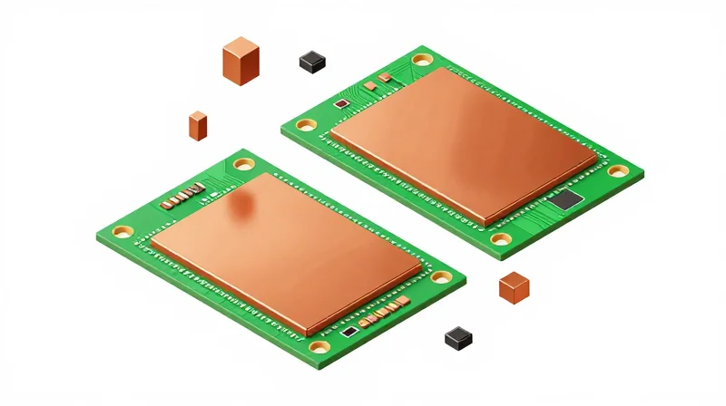
Strategic Grounding Topologies
The primary objective in load cell signal chain design is the preservation of the microvolt-level bridge output. A split-plane architecture is essential, where analog ground (AGND) and digital ground (DGND) are isolated to prevent high-speed return currents from circulating through sensitive analog reference nodes. While the planes must share a common reference point at the ADC to satisfy Kirchhoff’s Current Law, this connection should be established via a single, low-impedance bridge or star point to minimize crosstalk and ground bounce.
Plane Isolation and Return Path Management
Careless routing across split planes induces significant electromagnetic interference (EMI). If a digital trace must cross the split, it creates a large loop area for return currents, effectively acting as an antenna that broadcasts noise into the analog section. Designers must strictly enforce routing boundaries to ensure return currents follow the path of least impedance directly beneath the signal traces.
| Strategy | Benefit | Risk |
|---|---|---|
| Split Planes | Decouples noisy return paths from sensitive nodes | Risk of EMI if traces cross the split |
| Star Grounding | Eliminates ground loops | Increases routing complexity in dense boards |
| Continuous Planes | Lowest impedance path for high-speed signals | Potential for digital return noise injection |
Best Practices for Implementation
- How should I handle the ADC ground connection?
Connect the AGND and DGND pins of the ADC together at the device using a high-quality, low-impedance ground plane to prevent internal differential voltages. - Is a single ground plane ever preferable?
In highly integrated designs where routing is extremely constrained, a single continuous ground plane is often superior to a poorly executed split, provided that physical partitioning of components is strictly enforced. - What about high-speed digital signals near the load cell input?
Keep high-speed clocks and data buses at least 50 mils away from the analog front-end (AFE) signal paths and avoid routing them on layers adjacent to analog traces.
ADC Placement and Input Conditioning
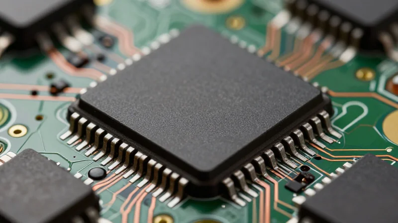
Optimizing ADC Proximity and Signal Path Integrity
The primary objective in high-precision load cell design is to minimize the distance between the bridge output and the ADC input. Every millimeter of trace length introduces potential for electromagnetic interference (EMI) pickup and increases susceptibility to trace resistance variations. By positioning the ADC immediately adjacent to the load cell connector, designers reduce the antenna area of the input traces and lower the parasitic capacitance that can compromise signal settling time.
Input Conditioning Best Practices
Effective signal conditioning requires a balanced approach to filtering. Placing a differential RC filter as close to the ADC pins as possible is mandatory to attenuate out-of-band noise and prevent aliasing. It is essential to use C0G/NP0 dielectric capacitors to avoid non-linear effects that could introduce distortion into the measurement.
| Design Element | Recommended Practice | Rationale |
|---|---|---|
| Trace Routing | Differential Pairs | Common-mode noise rejection |
| Component Selection | C0G/NP0 Capacitors | Superior stability and linearity |
| Filter Location | Adjacent to ADC | Minimized parasitic induction |
| Via Usage | Minimize counts | Reduction of impedance discontinuities |
Frequently Asked Questions
- Can I use standard X7R capacitors for input filtering?
No, X7R capacitors exhibit voltage and temperature coefficients that introduce significant non-linearity; always prioritize C0G/NP0 dielectrics for precision analog paths. - Why is differential routing crucial for load cells?
Load cell signals are inherently differential; routing them as tight, matched pairs ensures that common-mode interference is cancelled out at the ADC input stage. - Is it better to place the ADC near the processor or the sensor?
Always prioritize proximity to the sensor; digital signals are more robust over distance, whereas microvolt-level analog signals are highly prone to degradation.
Trace Impedance Control and Routing
Maintaining Differential Impedance Integrity
For high-precision load cell applications, differential signals must maintain a constant characteristic impedance—typically 90 or 100 ohms—across the entire signal path. Any deviation in trace geometry, spacing, or reference plane continuity results in impedance mismatches that cause signal reflections and degraded common-mode rejection ratios. Engineers must utilize controlled-impedance stackups and precise trace width calculations to ensure that the differential pair behaves as a balanced transmission line throughout the PCB layout.
Routing Best Practices to Minimize EMI
Routing sensitive analog traces requires a rigorous approach to geometry and loop area management. Loops created by improper return paths act as inductive loops that capture electromagnetic interference, while excessive trace lengths amplify capacitive coupling. Designers must adhere to strict length matching and avoid routing high-speed digital signals in proximity to the load cell input stage.
| Design Factor | Recommended Practice | Reasoning |
|---|---|---|
| Trace Symmetry | Equalize length and geometry | Maintains CMRR and signal balance |
| Via Usage | Minimize total via count | Reduces impedance discontinuities |
| Spacing | Wider than trace width | Reduces inter-pair crosstalk |
| Layer Transitions | Keep adjacent reference planes | Maintains stable return path inductance |
Common Routing Challenges FAQ
- Why should I avoid crossing gaps in the reference plane?
Crossing a gap forces the return current to take a longer, indirect path, significantly increasing the loop area and creating a high-inductance radiator that severely degrades signal integrity. - How does trace length matching affect precision?
Mismatched lengths induce phase shifts between the differential signals, turning common-mode noise into differential-mode noise that the ADC cannot cancel, directly impacting the effective bit resolution. - Is autorouting acceptable for precision sensor traces?
No; manual routing is essential to ensure that sensitive traces maintain the required clearances, avoid noisy digital planes, and remain in close proximity to their designated ground reference.
Mitigating Thermal Gradients in PCBA Layout

Addressing Thermal Impact on Load Cell Precision
Thermal gradients across a load cell PCBA induce uneven mechanical stress and thermoelectric voltages (Seebeck effect), which directly manifest as offset drift and instability. To achieve high-precision measurements, designers must isolate thermally sensitive analog circuitry from heat-generating components, such as power regulators, microcontrollers, and communication drivers.
Strategies for Thermal Isolation
- PCB Cutouts (Slots)
Mechanical milling or routing of slots between high-power digital sections and sensitive analog front-ends increases the physical thermal path resistance, effectively creating a thermal barrier. - Component Partitioning
Keep heat-dissipating components at the opposite end of the board from the precision excitation sources and bridge completion resistors to maintain a uniform temperature environment. - Copper Pours as Heat Spreaders
Use wide copper pours connected to internal planes to move heat away from sensitive components towards edge-mounted heatsinks or chassis grounds, preventing localized hot spots.
| Isolation Technique | Effectiveness | Design Complexity |
|---|---|---|
| PCB Cutouts | High (Physical Barrier) | Moderate (Structural Integrity) |
| Copper Heat Spreaders | Moderate (Thermal Averaging) | Low |
| Component Zoning | Very High (Source Reduction) | Low |
Best Practices for Thermal Management
Beyond physical separation, board layout must consider airflow and symmetry. Placing critical analog components along the same isothermal lines helps ensure that if the board heats up, the components drift in unison rather than differentially, which significantly reduces measurement errors.
Power Supply Decoupling for Low-Noise Performance
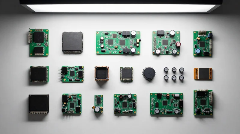
Decoupling Capacitor Hierarchy and Placement
To achieve superior signal integrity, a multi-tiered approach to power supply decoupling is essential. High-precision load cell conditioning circuits require low-impedance paths to ground to mitigate high-frequency noise and transient spikes. The fundamental rule is to place the smallest value capacitors (e.g., 10nF to 100nF) closest to the IC supply pins to provide an immediate reservoir of charge. Bulk capacitors (e.g., 10µF tantalum or ceramic) should be positioned further upstream to handle low-frequency ripple.
| Capacitor Type | Function | Placement Priority |
|---|---|---|
| 0.1µF Ceramic (X7R) | High-frequency noise shunt | Immediate (Closest to pin) |
| 10µF Tantalum/Electrolytic | Low-frequency bulk storage | Secondary (Near voltage regulator) |
| Ferrite Bead | EMI/RFI suppression | Series between supply and load |
Layout Best Practices for Minimizing Inductance
Parasitic inductance in power traces can invalidate even the best capacitor choices. Ensure the path from the capacitor to the ground plane is as short as possible, utilizing multiple vias if necessary to reduce loop area. Avoid routing power traces through multiple layers, which introduces via inductance that degrades high-frequency performance. A solid, contiguous ground plane directly beneath the decoupling network serves as the low-impedance return path necessary for stable measurements.
Frequently Asked Questions
- Why should I avoid using Vias-in-Pad for decoupling capacitors?
Vias-in-pad can result in uneven solder fillets and potential gas entrapment during reflow, leading to tombstoning or poor electrical connectivity, which ruins the decoupling effect. - Are electrolytic capacitors recommended for precision load cell power?
Avoid low-grade electrolytic capacitors as their high Equivalent Series Resistance (ESR) can fluctuate with temperature; instead, use low-ESR ceramic or tantalum capacitors for stable, temperature-consistent performance.
DFM Considerations for Automated Assembly
Automated assembly of high-precision load cell electronics demands strict adherence to DFM standards to prevent assembly-induced signal degradation. By aligning PCB layout practices with the mechanical constraints of pick-and-place equipment and reflow processes, designers can achieve superior yields while maintaining the structural integrity required for sensitive instrumentation.
Optimizing PCBA Layout for Automated Placement
Precision instrumentation requires stable component placement to avoid parasitic capacitance and mechanical stress. Standardizing footprint libraries and implementing robust panelization strategies are essential for high-throughput manufacturing.
| DFM Feature | Requirement for High-Precision | Benefit to Assembly |
|---|---|---|
| Fiducial Markers | Minimum 3 global markers | Enhanced registration accuracy |
| Component Clearance | At least 0.5mm edge-to-edge | Prevents solder bridging/shorts |
| Panelization | V-score with breakout tabs | Reduces stress-induced drift |
FAQ: Solving Common Assembly Challenges
- How do board cutouts for thermal isolation affect panelization?
Board cutouts reduce structural rigidity. Use strategic mouse-bites and robust peripheral rails to ensure the panel does not flex during pick-and-place, which prevents component misalignment. - Why is solder mask relief critical for load cell inputs?
Improper solder mask coverage can lead to leakage currents or inconsistent wetting. Define non-solder mask defined (NSMD) pads for precision components to improve solder joint reliability. - Can automated optical inspection (AOI) detect impedance issues?
AOI focuses on physical defects like misalignment or bridges. For impedance, you must verify via coupon testing or TDR (Time Domain Reflectometry) as part of the post-assembly quality process.
Recommendations for Signal Integrity Maintenance
To ensure that assembly does not compromise the precision of the load cell circuitry, avoid placing heavy components near the sensitive analog front-end. Ensure that all ground vias are capped or plugged where necessary to maintain consistent copper density, which aids in uniform heat distribution during the reflow process.
Testing and Validation of Signal Integrity
Post-Layout Signal Integrity Verification
Post-layout validation is the final safeguard against parasitic effects introduced during the PCB manufacturing process. For high-precision load cell applications, verification must extend beyond basic connectivity checks to include precise measurement of signal-to-noise ratios (SNR), common-mode rejection, and frequency response stability. Designers should utilize high-resolution digital multimeters and low-noise spectrum analyzers to correlate actual board performance with pre-layout electromagnetic simulation expectations.
Validation Techniques and Metrics
| Validation Technique | Primary Goal | Measurement Tool |
|---|---|---|
| Spectral Analysis | Identify periodic noise and interference spikes | FFT-capable Spectrum Analyzer |
| Noise Floor Characterization | Verify target resolution/bit count | High-Precision DMM / ADC |
| Step Response Analysis | Evaluate settling time and overshoot | Signal Generator / Oscilloscope |
FAQs on Load Cell Signal Validation
- How can I distinguish between sensor-induced noise and PCB-layout noise?
Measure the system with the load cell replaced by a low-noise metal-film precision resistor network. If the noise floor remains unchanged, the interference is likely coupled through the PCB layout or power supply rails. - What is the role of FFT analysis in signal verification?
Fast Fourier Transform (FFT) analysis is essential for identifying unintended frequencies in your signal chain, such as 60Hz hum, switching regulator harmonics, or clock feedthrough, which are often invisible in the time domain. - Is visual inspection sufficient for checking thermal isolation cutouts?
No. Visual inspection confirms placement, but you must perform thermal imaging or contact temperature probing under load to verify that the thermal isolation slots are effectively mitigating mechanical stress and thermal gradients.
Achieving high sensitivity in load cell designs requires a rigorous, disciplined approach to every layer of your PCBA layout. By prioritizing signal integrity through ground isolation, precision component placement, and EMI mitigation, you can turn a theoretical design into a production-ready instrument. Ready to elevate your hardware design? Contact our engineering team today to review your PCBA layout and optimize your sensor data acquisition for performance and reliability.
