
In the fast-paced evolution of ADAS, blind spot detection radar systems represent the pinnacle of automotive safety. However, designing for 77GHz millimeter-wave frequencies introduces severe signal integrity challenges. This guide provides an authoritative look at the DFM (Design for Manufacturing) standards required to transition from prototype to reliable, mass-produced automotive radar sensors.
Understanding Millimeter-Wave Signal Challenges

The Physics of Millimeter-Wave Challenges
At 77GHz, the wavelength of the signal is approximately 3.9mm. This scale means that standard PCB features such as vias, pad geometries, and even trace widths function as complex reactive components rather than simple conductors. Traditional design rules fail because they treat high-frequency signals as quasi-static currents, ignoring the wave-propagation characteristics and skin effect losses that dominate at millimeter-wave frequencies.
Key Impedance and Loss Constraints
| Challenge | Behavior at 77GHz | DFM Requirement |
|---|---|---|
| Dielectric Loss | High dissipation factor increases attenuation | Use ultra-low-loss PTFE or ceramic substrates |
| Skin Effect | Current flows only on the outer surface layer | Minimize surface roughness of copper foils |
| Via Discontinuity | Vias act as parasitic inductors and antennas | Implement via stitching and strict back-drilling |
Common Questions on Millimeter-Wave Design
- Why do standard FR-4 laminates fail in radar applications?
FR-4 exhibits high dielectric loss (Df) at 77GHz, causing signal attenuation that renders radar range measurements inaccurate and thermal instability that shifts the impedance profile. - How does surface roughness impact signal integrity?
At millimeter wavelengths, the skin depth is extremely shallow. Rough copper surfaces increase the path length for electron flow, leading to higher insertion loss and phase distortion. - What role does thermal management play in signal propagation?
Millimeter-wave dielectric constants are temperature-dependent; heat-induced fluctuations in the substrate alter the phase velocity, which directly compromises the angular resolution of blind spot detection sensors.
Selecting High-Frequency Laminates
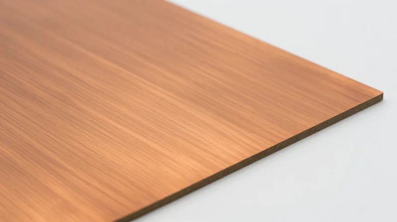
Critical Material Properties for 77GHz Radar
At automotive radar frequencies of 77GHz, traditional FR-4 materials are unsuitable due to high signal attenuation and dielectric instability. Designers must prioritize materials with a stable Dielectric Constant (Dk) across temperature ranges and an extremely low Dissipation Factor (Df). Achieving consistent performance in challenging automotive environments—ranging from -40°C to +125°C—relies on low moisture absorption and excellent thermal management properties.
Comparison of High-Frequency Substrate Characteristics
| Parameter | PTFE-based Laminate | Ceramic-Filled Hydrocarbon | LCP (Liquid Crystal Polymer) |
|---|---|---|---|
| Dk Stability | Excellent | Good | Very Good |
| Df (Loss) | Ultra-Low | Low | Very Low |
| Thermal Stability | High | High | Excellent |
| Cost Profile | Premium | Moderate | High |
Minimizing Insertion Loss: Copper Foil Selection
At mmWave frequencies, the skin effect restricts current flow to the outermost surface of the copper traces. Standard electrodeposited (ED) copper foil contains a high degree of surface roughness, which significantly increases insertion loss and alters the effective Dk. To mitigate these effects, designers should specify Very Low Profile (VLP) or Rolled Annealed (RA) copper foils, as smoother surfaces drastically reduce conductor losses in high-frequency transmission lines.
Selection FAQ
- How does Dk tolerance affect radar accuracy?
Variation in Dk directly impacts impedance control and phase velocity; even small deviations can cause beam-steering inaccuracies in radar sensors. - Is moisture absorption a significant factor?
Yes. Water has a high Dk (~80); moisture ingress into the laminate will shift the dielectric constant and degrade signal integrity over time. - Why is CTE matching important for 77GHz sensors?
The Coefficient of Thermal Expansion (CTE) must be closely matched to the copper foil to prevent trace cracking or delamination during extreme temperature cycling.
Strategic Layer Stack-up Design
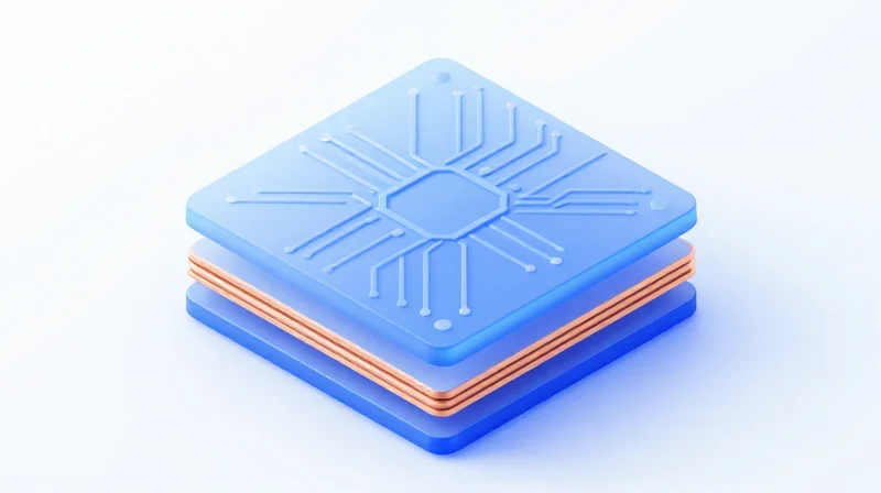
Optimizing Layer Stack-ups for High-Frequency Radar
Achieving optimal performance in automotive blind spot detection sensors requires a strictly symmetrical, low-loss stack-up design that prioritizes controlled impedance and minimized EMI. Because 77GHz signals are highly sensitive to layer transitions, designers must leverage thin dielectric cores and tightly coupled reference planes to suppress substrate modes and surface wave propagation.
Strategic Stack-up Configurations
| Feature | Design Strategy | Primary Benefit |
|---|---|---|
| Dielectric Thickness | Ultra-thin (under 4-5 mils) | Reduces dispersion and radiation loss |
| Ground Referencing | Solid adjacent planes | Prevents crosstalk and EMI leakage |
| Symmetry | Mirror-image construction | Minimizes board warpage during reflow |
Mitigating Electromagnetic Interference (EMI)
At millimeter-wave frequencies, the stack-up must function as an integrated Faraday cage. Designers should implement a 'G-S-G' (Ground-Signal-Ground) strip-line configuration wherever possible. This sandwich structure encapsulates the RF signal, preventing it from coupling with adjacent digital traces or power planes, which is vital for maintaining the strict signal-to-noise ratio required for reliable automotive detection.
Frequently Asked Questions
- Why is layer symmetry critical for radar sensors?
Asymmetrical stacks lead to coefficient of thermal expansion (CTE) mismatches, causing board warping that can physically alter the antenna pattern and performance at high frequencies. - How does via design affect the stack-up?
Vias create parasitic inductance; therefore, keep via stubs to an absolute minimum via back-drilling or buried via strategies to prevent impedance discontinuities at 77GHz. - Is hybrid stack-up design recommended?
Yes, using high-frequency PTFE-based laminates for the RF layer and standard FR-4 for non-critical control layers is a common cost-saving strategy, provided that the transition between materials accounts for CTE differences.
Precision Impedance Control Techniques
Mastering 50-Ohm Impedance at 77GHz
Maintaining a stable 50-ohm characteristic impedance is critical for 77GHz automotive radar systems to prevent signal reflections and minimize insertion loss. At millimeter-wave frequencies, the skin effect and surface roughness of copper become dominant variables. Designers must move beyond standard FR-4 calculations and adopt rigorous simulation-driven design processes that account for the anisotropic nature of high-frequency laminates.
Manufacturing Tolerance Management
Impedance variation is primarily driven by manufacturing tolerances in trace width and dielectric thickness. To ensure consistent signal performance across production batches, designers should specify a tolerance of +/- 5% for impedance-controlled nets and implement the following DFM strategies:
- Copper Weight Selection
Utilize thin copper foils (e.g., 0.5 oz or VLP/HVLP copper) to reduce side-etching effects, which significantly alter trace profiles and impedance calculations in narrow high-frequency lines. - Surface Finish Impact
Avoid HASL due to uneven topography. Opt for ENIG or ENEPIG, which provide a flat, uniform surface finish that minimizes parasitic capacitance and impedance discontinuities. - Etch Compensation
Coordinate directly with the board fabricator to apply specific etch-compensation factors, ensuring the final copper width at the board level matches the theoretical design requirement.
Geometry Comparison: Coplanar vs. Microstrip
| Feature | Microstrip | Grounded Coplanar Waveguide (GCPW) |
|---|---|---|
| High Frequency Performance | Moderate | Excellent |
| Crosstalk Suppression | Low | High |
| Manufacturing Sensitivity | High | Moderate |
| Application | General Signal Routing | Radar Front-end / Antenna Feeds |
For the sensitive radar front-end, Grounded Coplanar Waveguides (GCPW) are preferred. The proximity of adjacent ground planes provides better field containment, reducing radiation loss and minimizing the impact of dielectric variations. Always use TDR (Time Domain Reflectometry) testing coupons on every panel to verify that the manufactured impedance aligns with the targeted 50-ohm value before full-scale integration.
Advanced Trace Routing and Via Design
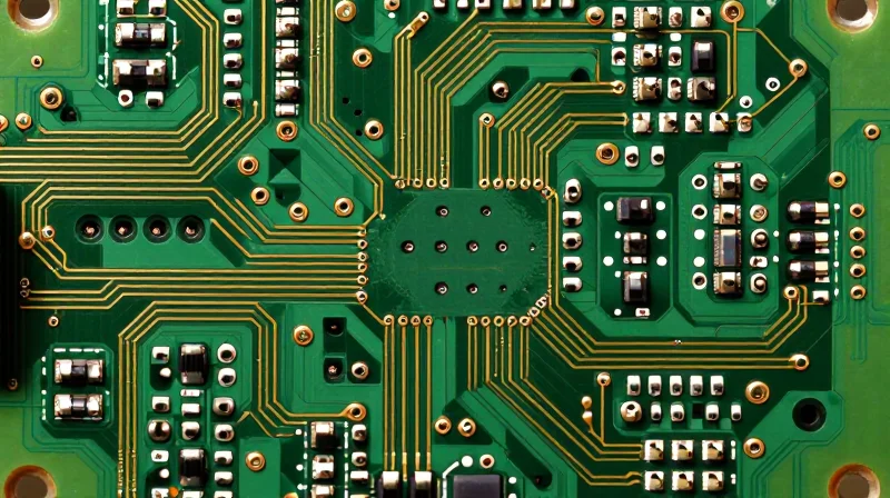
Advanced Micro-via and Routing Optimization
At 77GHz, every geometric discontinuity acts as an impedance mismatch, leading to significant signal reflection and attenuation. Advanced automotive radar design requires a transition strategy that minimizes parasitic capacitance and inductance associated with via structures. Designers must shift from standard through-hole transitions to high-density interconnect (HDI) micro-via technologies, specifically utilizing blind and buried vias with controlled stub lengths to prevent resonance phenomena.
Design Best Practices for High-Frequency Transitions
- Stub Elimination
Always employ back-drilling or blind vias to remove unused via stubs. Even a 0.5mm stub can behave as a quarter-wave resonator at 77GHz, causing severe signal suck-outs. - Ground Stitching
Place ground stitching vias within 0.2mm of signal transitions. This maintains a continuous reference return path and prevents the emergence of unintended cavity modes. - Pad Geometry
Implement teardrop pads on all trace-to-via connections to improve manufacturing yield and reduce the stress concentrations that lead to signal discontinuities.
| Feature | Standard PCB Practice | 77GHz Automotive Requirement |
|---|---|---|
| Via Type | Through-hole | Laser-drilled micro-via |
| Stub Management | None (Allowed) | Back-drilled or blind |
| Via Pitch | 0.8mm - 1.0mm | < 0.4mm for RF shielding |
| Routing | Standard orthogonal | Curvilinear / Tapered impedance transition |
Trace Geometry and Surface Roughness
The skin effect at 77GHz forces current to flow within a few micrometers of the copper surface. Therefore, the RMS roughness of the copper foil is a primary driver of insertion loss. Designers must specify 'Very Low Profile' (VLP) or 'Hyper-Low Profile' copper foils. Furthermore, trace corners should be mitered or rounded; sharp 90-degree bends produce excessive radiation and impedance spikes. Utilizing 'serpentine' routing with soft curves ensures that the characteristic impedance remains consistent throughout the routing path.
Mitigating Ground Bounce and EMI
Minimizing Ground Bounce in Radar Modules
Ground bounce, induced by rapid current surges during high-speed switching of RF components, can trigger false detections in blind spot sensors. To mitigate this, engineers must minimize the inductive loop area between the return path and signal traces. Implementing a solid reference plane directly adjacent to the top signal layer is mandatory to provide a low-impedance path for return currents.
Design Techniques for EMI Suppression
- Stitching Vias
Deploy an array of ground stitching vias around the periphery of high-speed RF sections to prevent lateral electromagnetic field radiation (edge leakage). - Isolated Islands
Avoid splitting ground planes under RF traces; if isolation is necessary between digital and analog sections, use a bridge at the connector point to prevent return path discontinuities. - Decoupling Strategy
Utilize low-ESL (Equivalent Series Inductance) capacitors mounted with minimal via-to-pad distance to suppress high-frequency noise transients at the power pins of the RF transceiver.
Comparative Analysis of Grounding Strategies
| Strategy | Primary Benefit | Impact on EMI |
|---|---|---|
| Solid Reference Plane | Minimized Inductance | High Reduction |
| Via Stitching | Contained RF Energy | High Reduction |
| Differential Pairs | Common Mode Rejection | Medium Reduction |
Best Practices for Automotive Compliance
To ensure compliance with CISPR 25 and automotive standards, designers must enforce strict physical separation between noisy DC-DC conversion circuitry and the sensitive 77GHz antenna feedlines. Use Faraday cage shielding techniques—incorporating conductive gaskets and perimeter via fences—to encapsulate the RF front-end, effectively isolating the module from external noise sources.
DFM for Mass Production Efficiency
Strategies for Maximizing Manufacturing Yield
In the context of automotive Blind Spot Detection (BSD) radar, transitioning from prototype to mass production requires a focus on DFM parameters that minimize variation. High-yield manufacturing hinges on panel-level efficiency and the reduction of manual handling during assembly. By standardizing component footprints and ensuring consistent copper balancing across the substrate, manufacturers can significantly lower the defect rate caused by thermal warping during reflow processes.
| Parameter | Prototypes | Mass Production Optimization |
|---|---|---|
| Panel Utilization | Single board focus | Nesting optimization for >85% yield |
| Component Pitch | Standard tolerance | Increased spacing for high-speed SMT |
| Copper Distribution | Functional only | Balanced copper planes to prevent warping |
Design for Automated Assembly and Inspection
For radar modules, automated optical inspection (AOI) and X-ray inspection are non-negotiable. To ensure these tools function effectively, designers must provide sufficient clearance for sensors and avoid crowding test points. Implementing fiducial markers correctly—both global and local—is essential for the high-precision alignment required by automotive-grade pick-and-place machines.
Frequently Asked Questions on DFM Efficiency
- How does copper balancing affect long-term reliability?
Uneven copper distribution creates thermal stress gradients that cause PCB warping during reflow, which can lead to solder joint fractures in vibrating automotive environments. - What is the role of fiducial markers in high-speed assembly?
Fiducials allow automated machines to compensate for microscopic shifts in the PCB panel, ensuring that high-frequency radar components are placed within the strict micron-level tolerances required. - Why should we avoid components near board edges?
Placing components close to the panel break line can lead to mechanical stress during depanelization, potentially damaging sensitive radar RF traces or decoupling capacitors.
Verification and Simulation Standards

The Role of EM Simulation in Pre-Production
For radar-based blind spot detection sensors, standard DRC (Design Rule Check) is insufficient. Engineers must utilize full-wave electromagnetic (EM) field solvers to analyze high-frequency signal integrity and antenna coupling before committing to physical prototyping. This pre-production simulation detects parasitic resonances and impedance discontinuities that standard EDA tools often overlook, ensuring that the sensor's radiation pattern remains within strict automotive specifications.
Simulation vs. Physical Testing
| Parameter | EM Simulation (Virtual) | Physical Testing (Hardware) |
|---|---|---|
| Phase | Pre-Prototype | Verification/Validation |
| Visibility | Internal Field Patterns | Measured Signal/EMI |
| Cost Impact | Low (Early Detection) | High (Re-spins required) |
Automotive Standards and Compliance
Automotive radar systems are governed by international safety and performance standards. Verification must be mapped against these requirements to ensure long-term reliability in harsh environmental conditions.
- ISO 26262 Compliance
Ensuring the PCB design supports functional safety requirements to prevent sensor failure during critical driving operations. - CISPR 25 Standards
Strict adherence to electromagnetic emission limits to ensure the sensor does not interfere with other vehicle electronic systems. - AEC-Q100/Q200
Validating that PCB materials and components meet thermal and mechanical stress requirements for automotive endurance.
Best Practices for DFM Validation
To close the loop on DFM validation, integrate Automated Optical Inspection (AOI) and X-ray inspection protocols into the manufacturing flow for the first article build. Correlating simulation data with real-world thermal camera results and vector network analyzer (VNA) measurements provides the final assurance required for high-volume automotive radar production.
By mastering these DFM principles, engineers can overcome the unique challenges of millimeter-wave radar and ensure high-performance, long-lasting automotive sensors. Are you ready to optimize your radar system for the next generation of autonomous driving? Contact our engineering team today to discuss your project requirements or to schedule a professional design review.
