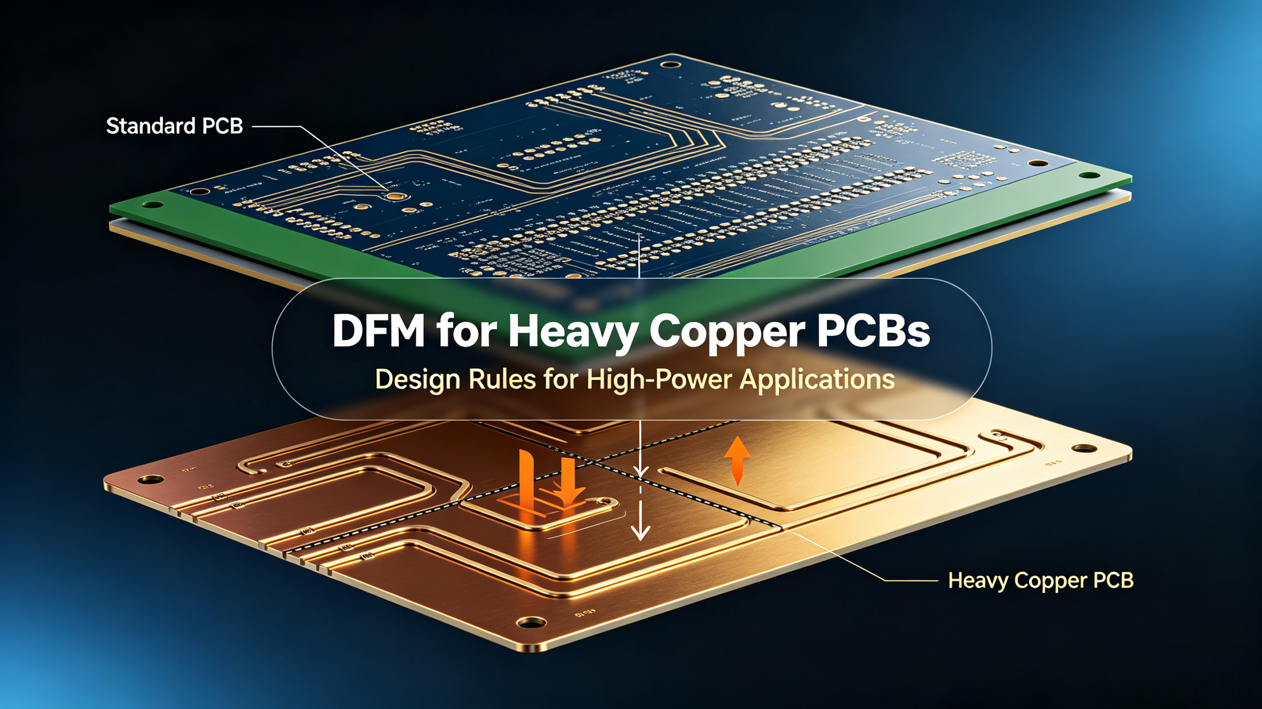
Most PCB designers are comfortable working with 1oz or 2oz copper. But when your design needs to handle high currents — think 20A, 50A, or more — you enter a different world. Heavy copper PCBs (generally defined as boards with 3oz or more of finished copper) are a different beast entirely.
What works for a standard board will fail on a heavy copper board. Etching behaves differently. Lamination is more difficult. Solder joints don't form the same way. And if you design without understanding these differences, your boards will come back with opens, shorts, or reliability issues that don't appear until the field.
This guide covers the essential DFM rules for heavy copper PCBs — written for engineers who need to get high-power boards manufactured reliably, the first time.
In the PCB industry, "heavy copper" typically refers to boards with 3oz or more of finished copper per layer. For reference:
| Copper Weight | Thickness (µm) | Typical Application |
|---|---|---|
| 1oz | 35µm | Standard signal boards |
| 2oz | 70µm | Medium power |
| 3oz | 105µm | Industrial power supplies |
| 6oz | 210µm | EV chargers, inverters |
| 10oz+ | 350µm+ | Extreme current applications |
Common heavy copper specs include 3oz, 4oz, 6oz, and 10oz, with some extreme designs going up to 14-20oz for specialized applications.
Heavy copper PCBs are used in:
Industrial power supplies and inverters
Electric vehicle charging systems and BMS
High-power LED lighting
Motor drives and servo controllers
Aerospace and defense power electronics
Heavy copper boards present several fundamental manufacturing challenges that standard PCBs don't:
Etching is not vertical. Copper etching is a chemical process that removes material in all directions, not just straight down. The thicker the copper, the more "undercut" (sideways etching) occurs. For heavy copper, this can mean 50% or more of the copper thickness is removed sideways.
Lamination is more difficult. Heavy copper traces are physically taller than standard traces (4-10x higher). This means more resin is needed to fill the gaps between traces during lamination. Standard prepreg often doesn't provide enough resin flow, leading to voids and delamination.
Soldering is a different process. Heavy copper planes act as heat sinks during reflow, absorbing heat from nearby pads. This can cause incomplete solder wetting, cold joints, and tombstoning if the thermal design isn't correct.
Drilling requires special consideration. Heavy copper layers are harder to drill through, cause faster tool wear, and require larger minimum hole sizes to ensure reliable plating.
The Problem: Heavy copper etching removes more material sideways than standard copper. If your traces are too narrow or too close together, they can disappear or bridge during etching.
The Rule of Thumb: Minimum trace width and spacing scale with copper thickness. A commonly cited rule is that the minimum trace width in mils should be approximately equal to the copper thickness in mils.
| Copper Weight | Minimum Trace Width (mm) | Minimum Spacing (mm) | Minimum Trace Width (mil) |
|---|---|---|---|
| 2oz | 0.2mm | 0.23mm | 8mil |
| 3oz | 0.3mm | 0.35mm | 12mil |
| 4oz | 0.4mm | 0.45mm | 16mil |
| 6oz | 0.6mm | 0.7mm | 24mil |
Note: These values are based on typical manufacturing capability. Always verify with your specific fabricator.
Etch compensation is essential. For 3oz copper, design trace width = target width + 0.1mm. For 6oz copper, add 0.2mm. Discuss etch compensation directly with your manufacturer — they may have specific rules based on their equipment.
Avoid narrow traces on heavy copper layers. On 6oz copper, traces narrower than 1mm are problematic for most manufacturers. If you need fine-pitch routing, consider using a mixed copper stackup.
The old IPC-2221 standard significantly underestimates current capacity for heavy copper. The newer IPC-2152 standard provides more accurate models based on empirical data and should be your reference for heavy copper designs.
Current Capacity Table (30°C rise, still air):
| Trace Width | 3oz Current | 6oz Current | 10oz Current |
|---|---|---|---|
| 100 mil | 12A | 19A | 28A |
| 200 mil | 20A | 32A | 47A |
| 500 mil | 38A | 62A | 91A |
| 1000 mil | 62A | 101A | 148A |
Data from IPC-2152 standard. External layers carry approximately 20-30% more current due to convection cooling.
Via Diameter: Standard via sizes often fail on heavy copper boards. The hole wall copper must match the thick outer copper, requiring larger minimum via diameters.
Minimum via diameter for heavy copper:
3oz: ≥0.8mm (≥0.9mm recommended)
6oz: ≥1.0mm
10oz: ≥1.2mm
Multiple vias for high current. Do not rely on a single via to carry high current. A 3oz copper trace carrying 5A should use 2-3 vias in parallel (each via can handle ~2-3A).
Via-in-pad is risky. If you must use via-in-pad on heavy copper boards, specify filled and capped vias (IPC-4761 Type VII). Without filling, solder will wick down the via barrel during reflow, starving the joint.
Heavy copper spreads heat across the board. The thermal benefit of heavy copper comes from both increased thickness (lower thermal resistance) and the ability to spread heat over a larger area.
| Construction | Temperature Rise (5W component, no airflow) |
|---|---|
| 1oz copper, 20mm² spread | ~45°C |
| 3oz copper, 50mm² spread | ~18°C |
| 6oz copper, 100mm² spread | ~8°C |
| 6oz + thermal via array | ~5°C |
Data from AtlasPCB thermal analysis
Use thermal relief connections. Always use thermal relief spokes (typically 8-12mil wide) to connect vias and pads to heavy copper planes. Without thermal relief, the massive copper heat sink will make soldering nearly impossible.
One of the most important principles in heavy copper design is that you don't need heavy copper on every layer — and often, you shouldn't use it everywhere.
Mixed copper construction means using heavy copper on power/ground planes and standard copper on signal layers. This approach provides the best balance of current capacity, signal routing density, and manufacturability.
Typical mixed stackup for a 6-layer board:
Layer 1 (Top): 2oz — Signal + component pads
Layer 2 (Inner): 6oz — Power plane (high current)
Layer 3 (Inner): 6oz — Ground plane (return current + heat spreading)
Layer 4 (Inner): 1oz — Signal routing
Layer 5 (Inner): 1oz — Signal routing
Layer 6 (Bottom): 2oz — Signal + component pads
Key DFM consideration: Mixed copper creates lamination challenges. Different copper weights create asymmetric stress during lamination. Your stackup should be copper-balanced around the center axis to prevent warping. High-resin-content prepreg is required adjacent to heavy copper layers to fill the gaps between traces.
Solder mask on heavy copper needs special attention. Thick copper traces have tall sidewalls that resist uniform mask coverage. Standard mask application often results in thin spots or peeling during soldering.
Recommended practices:
Request multiple solder mask passes (2-3 passes) for heavy copper boards
Consider mask relief for tall copper features
Verify your fabricator uses an LPI solder mask designed for heavy-copper boards
Layer stackup must be symmetrical. Heavy copper layers should be balanced above and below the board center to prevent warpage. For example, if you have a 6oz plane on Layer 2, you should have a 6oz plane on Layer 5 or 7.
Board thickness can be a challenge. Heavy copper boards are thicker than standard PCBs. Factor this into connector selection and enclosure design.
Annular ring must be larger. With the looser registration tolerances and increased thermal stress of heavy copper, annular ring should be at least 8-10mil (0.20-0.25mm) on inner and outer layers. For high-current or plated-through holes, specify 12mil or more.
When documenting a heavy copper PCB design for manufacturing, avoid these common errors:
Mistake 1: Not specifying finished vs starting copper weight — this creates a 30-50% thickness discrepancy.
Mistake 2: Using standard trace/space rules on heavy copper layers — this causes opens and shorts.
Mistake 3: Forgetting etch compensation in impedance calculations — the trapezoidal profile of heavy copper traces changes impedance.
Mistake 4: Direct plane connections without thermal relief — this creates unmanufacturable solder joints.
Mistake 5: Missing specification for high-resin-content prepreg — standard prepreg can't fill heavy copper gaps.
When you send a heavy copper PCB for fabrication, your manufacturing notes should include:
HEAVY COPPER SPECIFICATION:
- Copper weight on each layer: _____ oz (finished)
- Minimum trace/space on heavy copper layers: ____/____ mil
- Minimum via: ____ mil finished hole, ____ mil pad
- Thermal relief spoke width: ____ mil
- Soldermask: Multiple pass, LPI type
- Etch compensation: _____ mil
- IPC-6012 Class 2 (or Class 3 for high-reliability)
- Cross-section verification required on first article
Heavy copper PCBs enable high-power, high-current designs that standard boards cannot support. But they require a different design mindset from the start.
Three keys to success:
Widen everything — traces, spaces, vias, and annular rings all need to be larger than you're used to
Design for thermal relief — heavy copper conducts heat, so plan for soldering challenges
Use mixed copper when possible — heavy copper on power layers, standard copper on signal layers
If you're planning a heavy copper design, start the conversation with your manufacturer early. Share your stackup and minimum feature sizes before you commit to layout — the earlier you catch DFM issues, the cheaper they are to fix.
???? www.anypcba.com/contact-us/
???? We specialize in small-to-medium batch PCB and PCBA — from prototypes to production. If you're designing a heavy copper board and need a DFM review, send us your files. We'll check it against our manufacturing capabilities and give you a transparent quote.




