 Introduction
You've spent weeks designing your PCB. The layout is complete. You send the files to your manufacturer with confidence.
Then the boards come back — and half of them don't work.
This is where PCB testing comes in. A proper testing strategy is the difference between catching defects early and finding them in the field. As one PCB manufacturer puts it, a tiny solder bridge that's invisible to the naked eye can turn your masterpiece into an expensive coaster. That's why PCB testing exists.
This guide covers the full spectrum of PCB testing methods — from bare board verification to functional testing — and helps you choose the right strategy for your project.
The cost of catching a defect scales dramatically with when you find it:
| When Defect Is Found | Cost Impact |
|---|---|
| During bare board fabrication | Low — scrap or rework before assembly |
| During factory testing | Medium — labor + components + rework |
| In the field | Extremely high — returns, replacements, lost trust, warranty claims |
The "10x rule" is a well-known principle in manufacturing: a defect caught at the next stage costs roughly 10x more to fix. A problem caught during bare board testing might cost pennies. The same problem found in the field can cost hundreds or thousands of dollars — plus damage to your brand reputation.
Every PCB should be electrically verified before any components are placed.
This checks that the bare board has the correct connections — no opens (connections that should exist but don't) and no shorts (connections that shouldn't exist but do).
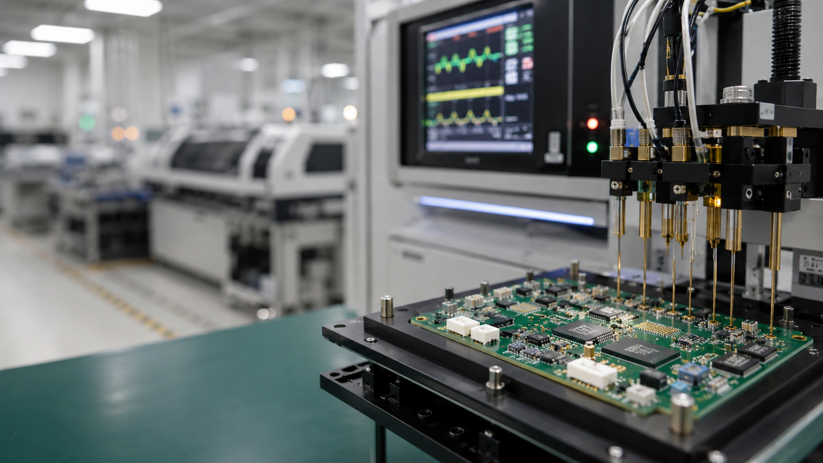
Flying Probe Testing:
Motor-driven probes move across the board
Tests each net for continuity and isolation
No fixture required — ideal for prototypes and small batches
Speed: 5-50 test points per second
Cost: $0.50-5.00 per board depending on complexity
Fixture Testing (Bed-of-Nails):
Spring-loaded probes on a custom fixture contact all test points simultaneously
Very fast — seconds per board
Fixture cost: $500-3,000 (amortized across production volume)
Best for: Medium to high volume (>500 pieces)
For controlled impedance boards, Time Domain Reflectometry (TDR) verifies that impedance values meet specifications. Test coupons on the panel edge are measured and recorded.
These tests happen during the assembly process and catch defects before they propagate downstream.
SPI checks solder paste deposits before components are placed, and it's important because roughly 60% of SMT defects originate in the solder paste printing process.
SPI measures:
Solder paste volume, height, and area
Offset and bridging
AOI uses high-resolution cameras to inspect assembled boards after reflow, comparing images against expected component placement and solder joint appearance.
What AOI catches:
Missing or misoriented components
Component shift or tombstoning
Solder bridges or insufficient solder
Wrong component markings
What AOI misses:
Incorrect component values (a 10K and 100K resistor look identical)
Hidden defects under BGAs
Functional failures
Internal IC damage
X-Ray inspection is essential for joints that optical inspection cannot see — specifically BGAs, QFNs, and other hidden solder joints.
2D X-Ray: Fast inspection showing a projection image of the board. Good for detecting bridges and voids.
3D CT (Computed Tomography): Provides layer-by-layer 3D reconstruction — can pinpoint the exact defective ball on a BGA.
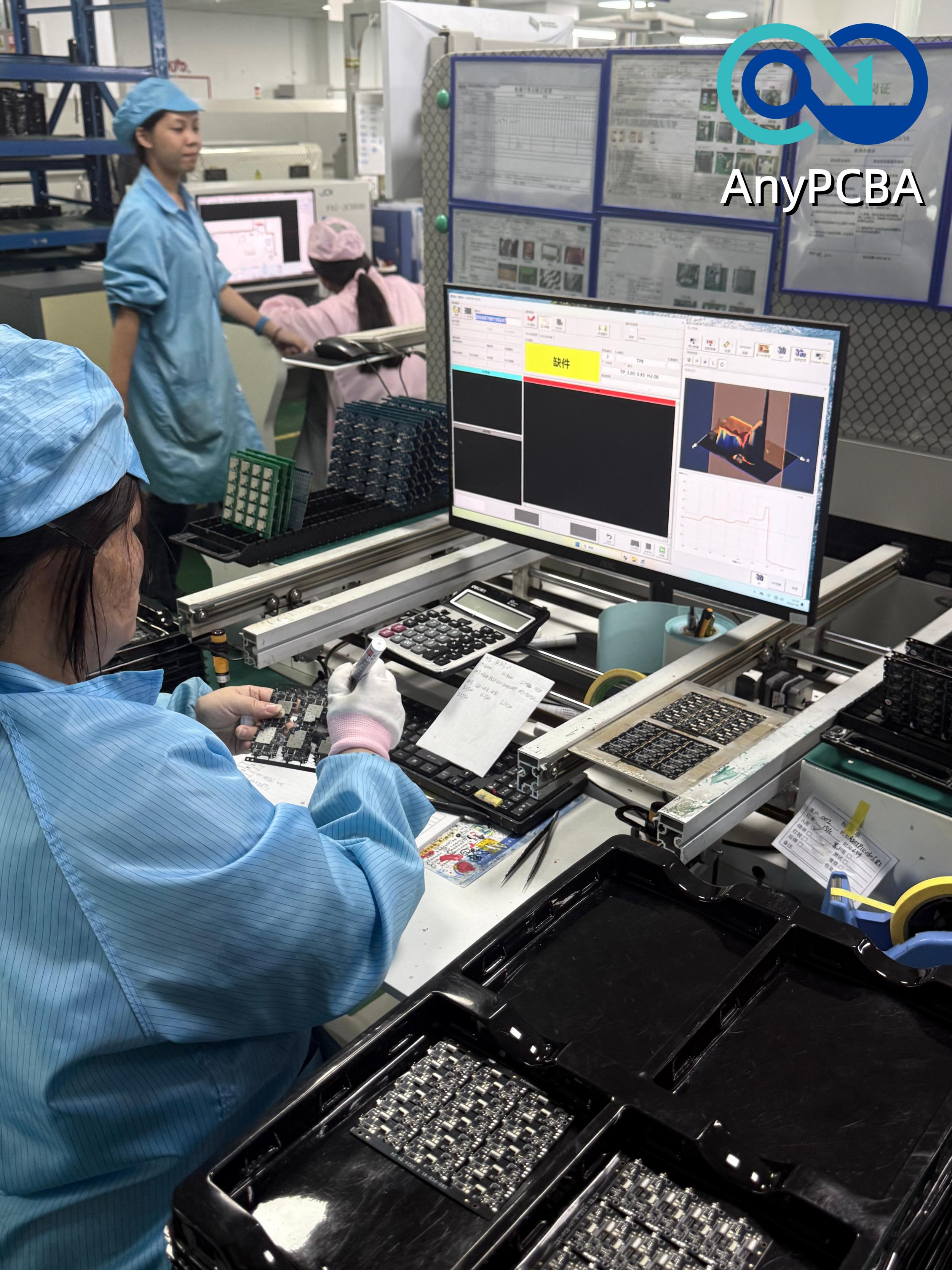
ICT uses a bed-of-nails fixture to contact test points on the assembled board, measuring electrical characteristics.
What ICT catches:
Component values (e.g., 10K vs 100K resistors)
Diode/transistor polarity and forward voltage
IC pin connectivity
Shorts and opens
Power supply voltages
Advantages:
High fault coverage (>95%)
Tests electrical properties, not just appearance
Fast — 10-30 seconds per board
Disadvantages:
Requires custom fixture ($3,000-15,000)
Requires test points on the board
Not suitable for prototypes or small batches
FCT powers up the board and verifies it operates correctly in its intended application. This is the only test that confirms the board actually works.
FCT typically verifies:
Power supply voltages
Communication interfaces (UART, SPI, I2C, USB, Ethernet)
Sensor readings
LED and display operation
Motor or actuator control
Firmware programming and verification
Two IPC standards form the foundation of PCB testing:
IPC-6012 — Performance specification for rigid PCBs. Defines minimum quality requirements for bare boards before assembly, covering:
Conductor width/spacing tolerances
Plating thickness
Via quality and hole wall integrity
Solder mask accuracy
IPC-A-600 — Acceptability of printed boards. Defines what a finished board should look like, with acceptable vs. defect examples.
For assemblies, IPC-A-610 defines acceptability criteria for PCBA.
| Production Volume | Recommended Testing | Why |
|---|---|---|
| Prototypes (1-50) | Flying probe + Functional testing | No fixture costs, flexible, catches design issues |
| Small batch (50-500) | Flying probe + AOI + Functional testing | Good coverage without heavy fixture investment |
| Medium batch (500-5,000) | ICT + AOI + X-Ray (spot) + Functional (sample) | Fixture cost amortized, high fault coverage |
| High volume (5,000+) | ICT + AOI + X-Ray + Functional (sample) | Maximum coverage, lowest per-board cost |
Key principle: No single test catches all defects. The most effective PCB testing strategy is layered — different tests catch different types of problems at different stages. A board that passes AOI can still have a wrong-value resistor. A board that passes ICT can still fail in the field due to firmware issues. Functional testing is the only way to know the board works as intended.
| Test Method | Stage | Catches | Best For |
|---|---|---|---|
| Flying Probe | Bare board | Opens, shorts | Prototypes, small batches |
| Fixture (ICT) | Bare board / Assembled | Opens, shorts, components | High volume |
| SPI | Before placement | Solder paste defects | All volumes |
| AOI | After reflow | Visual defects, placement | All volumes |
| X-Ray | After reflow | BGA, hidden solder joints | BGA-heavy designs |
| ICT | Assembled | Component values, connections | Medium-high volume |
| Functional Test | Final | Actual operation | Every board |
???? www.anypcba.com/contact-us/
???? We test every board we build. From flying probe to functional test — because we want your boards to work when they arrive.




