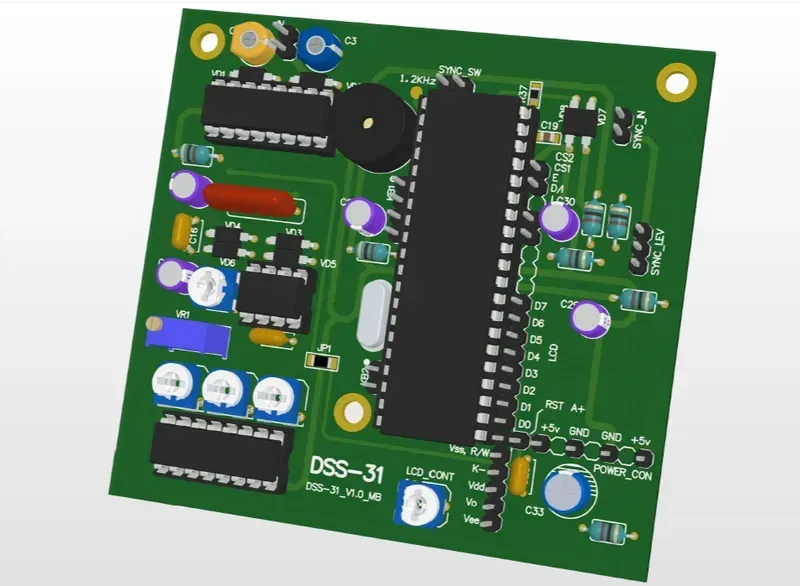
In today's rapidly evolving electronics industry, the digital oscilloscope stands as an indispensable tool for engineers and technicians. Its ability to visualize and analyze electrical signals in real-time is crucial for debugging, testing, and validating electronic designs. At the heart of every digital oscilloscope lies a Printed Circuit Board (PCB), a critical component that dictates the instrument's performance, reliability, and accuracy. Zero One Solution Limited understands the significance of a well-designed PCB in achieving optimal oscilloscope functionality. We provide comprehensive PCB solutions tailored specifically for digital oscilloscopes, empowering engineers to push the boundaries of innovation. From high-speed signal integrity to meticulous component placement, our expertise ensures your oscilloscope performs at its peak. This article delves into the intricacies of digital oscilloscope PCB solutions, exploring the challenges, design considerations, and manufacturing processes that underpin a successful oscilloscope design.
Understanding the Critical Role of PCBs in Digital Oscilloscopes
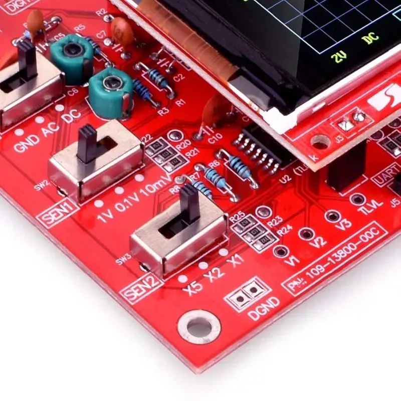
Oscilloscope PCB Board
The Printed Circuit Board (PCB) serves as the foundational backbone of any digital oscilloscope, dictating its precision, bandwidth, and overall measurement accuracy. Far more than just a connection medium, the PCB's design, material, and fabrication directly impact signal integrity, noise rejection, and the faithful representation of high-frequency waveforms. A meticulously engineered PCB is paramount to achieving the rigorous performance standards expected from modern digital oscilloscopes, particularly in applications demanding high-resolution and low-noise measurements.
Signal Integrity and High-Frequency Performance In digital oscilloscopes, PCBs must manage extremely high-frequency signals with minimal distortion. This demands precise impedance control, careful trace routing to avoid reflections and crosstalk, and optimized layer stack-up to maintain signal fidelity across wide bandwidths. Compromised signal integrity at the PCB level translates directly into inaccurate readings and reduced measurement capabilities.
Noise Reduction and Electromagnetic Compatibility (EMC) Digital oscilloscopes operate in environments susceptible to various forms of electrical noise and electromagnetic interference (EMI). The PCB design plays a critical role in mitigating these disturbances through effective grounding strategies, power plane design, and component placement that minimizes parasitic capacitance and inductance, thereby ensuring clean signal acquisition.
Thermal Management for Sustained Accuracy High-performance digital oscilloscopes often integrate complex ASICs, FPGAs, and high-speed ADCs that generate significant heat. The PCB must be designed to effectively dissipate this heat, preventing thermal drift that can degrade measurement accuracy and long-term reliability. This involves strategic use of thermal vias, copper pours, and consideration of PCB material's thermal properties.
Power Delivery Network (PDN) Stability A stable and low-noise power delivery network is crucial for the sensitive analog and digital circuits within an oscilloscope. The PCB's PDN design, including decoupling capacitor placement and power plane impedance, directly influences the stability of voltage rails and the reduction of power supply noise, which can otherwise couple into sensitive signal paths.
Miniaturization and Density Challenges Modern oscilloscopes are increasingly compact, demanding high component density on the PCB. This necessitates advanced PCB manufacturing capabilities, such as fine-line etching, microvias, and HDI (High-Density Interconnect) technology, to accommodate complex circuitry within limited spatial constraints without compromising performance.
Key Challenges in Digital Oscilloscope PCB Design
Designing Printed Circuit Boards (PCBs) for digital oscilloscopes presents a unique set of formidable challenges that demand precision engineering and a deep understanding of high-frequency electronics. Unlike general-purpose PCBs, oscilloscope PCBs must reliably process signals spanning gigahertz frequencies, maintain signal integrity with picosecond-level accuracy, and suppress noise across a broad spectrum. The core difficulties lie in managing high-speed signal propagation, ensuring stringent impedance control, mitigating thermal accumulation, and safeguarding against electromagnetic interference (EMI), all of which are paramount for the instrument's accuracy and performance.
High-Speed Signal Routing Complexity Digital oscilloscopes operate with extremely high bandwidths, meaning signals with very fast rise times. Routing these high-speed signals requires meticulous attention to trace length matching to prevent skew, controlled impedance to minimize reflections, and careful consideration of via structures to avoid parasitic capacitance and inductance, which can degrade signal integrity and introduce errors into measurements. This necessitates advanced routing strategies and simulation tools to predict and mitigate issues before fabrication, ensuring signal fidelity across multiple layers and complex interconnects.
Signal reflections, waveform distortion, data loss
Trace width/spacing, dielectric constant of material, stack-up design
Power Delivery Network (PDN)
Voltage drops, ground bounce, increased noise
Decoupling capacitors, low-inductance power planes, clean power rails
Addressing these multifaceted challenges requires a holistic design approach, integrating advanced materials, sophisticated layout techniques, and rigorous validation processes. The selection of low-loss dielectric materials, meticulous stack-up design, and precise manufacturing tolerances are all critical to achieving the required performance. Furthermore, effective thermal management is vital, as excessive heat can compromise component stability and drift performance. Zero One Solution Limited leverages its extensive expertise in high-frequency PCB design and manufacturing to navigate these complexities, ensuring that the PCBs underpinning digital oscilloscopes meet the stringent demands for accuracy, reliability, and long-term stability.
High-Speed PCB Layout Techniques for Optimal Signal Integrity
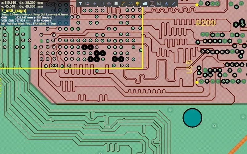
High-Speed PCB Layout
Achieving optimal signal integrity is paramount in digital oscilloscope PCB design, as even minor signal degradation can compromise measurement accuracy. High-speed PCB layout techniques are not merely best practices but critical engineering disciplines that directly impact an oscilloscope's performance by minimizing signal distortion, reflections, and crosstalk, thereby ensuring the faithful capture and display of complex waveforms. Strategic implementation of these techniques is essential for maintaining the fidelity of high-frequency signals traversing the PCB.
Trace Impedance Matching Maintaining controlled impedance throughout signal paths is fundamental. Mismatched impedance causes reflections, leading to signal ringing and distortion. This involves carefully calculating trace width, dielectric constant, and distance to reference planes. For common 50-ohm or 75-ohm characteristic impedance, precise control is achieved through simulation and strict manufacturing tolerances, often requiring specialized materials and stack-ups.
Minimizing Stubs and Via Usage Stubs, or unterminated trace lengths, act as antennas at high frequencies, creating reflections and signal loss. They should be avoided or kept as short as possible. Similarly, vias introduce impedance discontinuities and inductance, which degrade signal integrity. Minimizing via count, especially on critical high-speed traces, and using blind or buried vias where possible, helps preserve signal quality by providing cleaner return paths and reducing parasitic effects.
Optimized Layer Stack-up A well-designed layer stack-up provides stable power and ground planes, crucial for controlled impedance and noise suppression. Multiple ground layers sandwiching signal layers create effective shielding and clear return paths. For high-speed designs, a typical stack-up might include signal layers adjacent to ground planes, providing tight coupling and minimizing loop inductance. This also aids in containing electromagnetic fields and reducing EMI.
Differential Pair Routing For high-speed differential signals, maintaining tight coupling and equal length within the pair is critical to preserve common-mode noise rejection and signal integrity. Routing differential pairs with controlled spacing and ensuring symmetrical return paths prevents skew and mode conversion, which are detrimental to high-speed data transmission in digital oscilloscopes.
Grounding and Decoupling Strategies Robust grounding, often through solid ground planes, provides a low-impedance return path for signals and minimizes ground bounce. Strategic placement of decoupling capacitors close to IC power pins reduces transient noise and ensures stable power delivery, particularly for high-speed digital and analog components, preventing voltage fluctuations that can corrupt sensitive measurements.
Component Selection and Placement for Reduced Noise and Interference
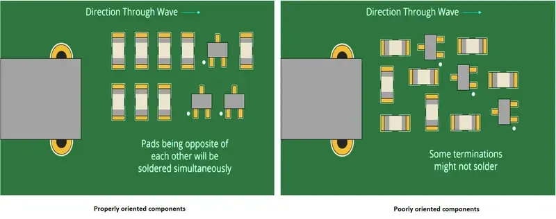
PCB Component Placement
Optimizing component selection and placement is paramount in digital oscilloscope PCB design to effectively mitigate noise and electromagnetic interference (EMI). The strategic choice of components, coupled with their precise layout on the PCB, directly impacts the instrument's sensitivity, accuracy, and overall signal integrity, ensuring that the acquired waveforms are true representations of the input signals without unwanted artifacts. This meticulous approach is critical for achieving the high-performance standards demanded by advanced digital oscilloscopes.
Critical Component Selection Criteria Selecting the right components is the first line of defense against noise and EMI. For digital oscilloscopes, this involves prioritizing components with low noise figures, high linearity, and appropriate frequency response. Key considerations include: highly stable voltage regulators to ensure clean power rails; low-ESR (Equivalent Series Resistance) capacitors for effective power supply decoupling and ripple reduction; high-bandwidth operational amplifiers with low input noise voltage and current; and carefully chosen high-speed logic ICs with controlled rise/fall times to minimize switching noise. The parasitic characteristics (inductance, capacitance, resistance) of each component must be thoroughly evaluated to understand their impact on signal integrity at the operating frequencies of the oscilloscope.
Strategic Component Placement Techniques Once selected, the placement of these components on the PCB is equally vital. Proper placement minimizes trace lengths, reduces loop areas, and facilitates effective shielding, all of which contribute to reduced noise and interference. Key strategies include: segregating analog and digital sections to prevent digital switching noise from contaminating sensitive analog front-ends; placing decoupling capacitors as close as possible to the power pins of ICs to provide immediate charge and suppress transient voltage fluctuations; orienting components to minimize inductive coupling; creating dedicated ground planes for sensitive circuits to provide a low-impedance return path for signals; and positioning high-power or high-frequency components away from sensitive measurement paths to prevent thermal and electromagnetic crosstalk. Effective heat dissipation from power-consuming components must also be considered during placement to maintain operational stability and component longevity.
Component Type
Noise Reduction Strategy
Placement Guideline
Voltage Regulators
Low noise, high PSRR (Power Supply Rejection Ratio)
Close to power-consuming ICs, isolated from sensitive analog circuits
Decoupling Capacitors
Low ESR, appropriate capacitance for frequency
Directly adjacent to IC power pins, multiple capacitors for different frequencies
High-Speed Amplifiers
Low input noise, high slew rate, wide bandwidth
Near input connectors, minimal trace length to analog-to-digital converters (ADCs)
Digital ICs
Controlled rise/fall times, low quiescent current
Grouped in digital sections, away from analog components, proper ground connections
Connectors & Filters
Shielded, common-mode choke/EMI filters
At board entry/exit points, maintaining signal integrity from external sources
Thermal Management Strategies for High-Performance Oscilloscope PCBs
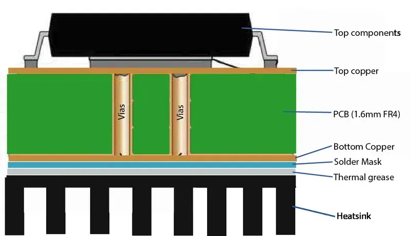
PCB Heat Sink
Effective thermal management is paramount for the long-term reliability and accurate performance of high-performance digital oscilloscope PCBs. Heat generated by densely packed, high-speed components can significantly degrade signal integrity, shorten component lifespan, and even lead to operational failure. Implementing robust thermal strategies ensures that critical components operate within their specified temperature ranges, preserving measurement precision and system stability.
Heat Sinks and Fans Heat sinks, often made of aluminum or copper, are designed to increase the surface area for heat dissipation, drawing heat away from critical components like ADCs, FPGAs, and microprocessors. When passive heat sinks are insufficient, active cooling solutions like forced-air fans are integrated to enhance airflow and heat removal, particularly in compact or high-power designs.
Thermal Vias and Copper Pours Thermal vias are plated through-holes that connect hot components to internal copper planes, acting as efficient heat conduits to distribute thermal energy across multiple PCB layers. Large copper pours on ground and power planes also serve as effective heat spreaders, leveraging the high thermal conductivity of copper to dissipate heat more uniformly across the board, preventing localized hotspots.
Optimized Component Placement Strategic component placement is a foundational thermal management technique. Heat-generating components should be distributed evenly across the PCB to avoid thermal crowding. High-power components should be placed near the edges of the board or closer to airflow paths, and away from sensitive analog circuitry to prevent thermal interference and maintain signal integrity. Considerations include grouping components with similar thermal profiles and ensuring sufficient spacing.
Material Selection for Enhanced Thermal Performance The choice of PCB substrate material significantly impacts thermal dissipation. Materials with higher thermal conductivity, such as certain FR-4 variants or specialized laminates, can facilitate more efficient heat transfer away from active components. Zero One Solution Limited advises on selecting appropriate materials that balance thermal performance with electrical requirements and cost considerations for optimal oscilloscope PCB designs.
Thermal Modeling and Simulation Advanced thermal modeling and simulation tools are crucial for predicting temperature profiles and identifying potential hotspots early in the design cycle. By simulating various operating conditions and cooling strategies, engineers can optimize component layout, define appropriate heat sink requirements, and validate thermal management designs before physical prototyping, minimizing costly redesigns and accelerating time-to-market. This predictive analysis ensures the thermal integrity of the final product.
Manufacturing Considerations for High-Precision Oscilloscope PCBs
PCB Etching
The manufacturing phase is as crucial as design in determining the ultimate performance and reliability of high-precision digital oscilloscope PCBs. Achieving the stringent requirements for signal integrity and noise reduction necessitates meticulous attention to material selection, precise etching, and optimal surface finishes. These considerations are paramount for ensuring that the theoretical design translates into a functionally superior and durable product, capable of accurate signal acquisition in demanding environments.
Material Selection: The Foundation of Performance The choice of substrate material directly impacts signal propagation speed, impedance control, and thermal dissipation. For high-frequency oscilloscope PCBs, low-loss dielectric materials such as specialized FR-4 variants, Rogers, or PTFE-based laminates are critical. These materials exhibit stable dielectric constants (Dk) and low dissipation factors (Df) across wide frequency ranges, minimizing signal loss and dispersion. For instance, a typical Rogers 4350B material offers a Dk of 3.66 and a Df of 0.0037 at 10 GHz, significantly outperforming standard FR-4 for high-speed applications. The material's thermal properties are equally important to manage heat generated by high-density components, preventing performance degradation and extending operational lifespan. Considerations also extend to copper foil type and thickness, with electro-deposited (ED) copper being standard, but rolled annealed (RA) copper preferred for very high-frequency designs due to its smoother surface, which reduces skin effect losses.
Zero One Solution Limited: Your Partner for Digital Oscilloscope PCB Solutions
At Zero One Solution Limited, we understand the intricate demands of Digital Oscilloscope PCB Solutions. Our specialized expertise in rapid prototyping, combined with a comprehensive one-stop service from design to manufacturing and assembly, positions us as the ideal partner for developing high-performance oscilloscope PCBs that meet the most stringent signal integrity and reliability requirements. Leveraging our strategic global presence and deep industry knowledge, we empower innovation and accelerate your time-to-market.
Comprehensive Design and Engineering Support Our seasoned engineers provide end-to-end design support, focusing on high-speed signal routing, impedance control, and noise reduction critical for digital oscilloscopes. We optimize layer stack-up, component placement, and thermal management to ensure superior performance and longevity.
Rapid Prototyping and Iteration With a core focus on rapid-response R&D prototype manufacturing, Zero One Solution Limited significantly reduces development cycles. Our agile processes allow for quick iterations and rigorous testing, ensuring your oscilloscope PCB designs are validated efficiently and accurately.
Advanced Manufacturing Capabilities Utilizing state-of-the-art manufacturing facilities, we ensure precision in every aspect of PCB production. From meticulous material selection (e.g., low-loss laminates) to advanced etching accuracy and diverse surface finishes, our processes guarantee the highest quality and reliability for your digital oscilloscope PCBs.
Seamless Assembly and Testing Beyond manufacturing, we offer comprehensive PCB assembly (PCBA) services, including precise component mounting (SMT/THT), rigorous functional testing, and quality assurance. Our integrated approach ensures that the assembled PCBs meet all design specifications and performance benchmarks, ready for seamless integration into your digital oscilloscopes.
Global Supply Chain and Local Expertise Headquartered in Shenzhen, China, and with a branch in Dubai, Zero One Solution Limited operates strategically within a global PCBA supply chain network. This unique positioning provides unparalleled access to resources, enabling us to deliver cost-effective solutions without compromising on quality or lead times.
Streamlines production and guarantees functionality
Global Logistics & Support
Strategic locations in Shenzhen & Dubai, worldwide network
Access to global resources, competitive pricing, efficient delivery
Case Studies: Successful Digital Oscilloscope PCB Projects
Digital Oscilloscope PCB Project
At Zero One Solution Limited, our commitment to excellence in PCB solutions for digital oscilloscopes is best demonstrated through tangible successes. These case studies highlight our capability to address complex design and manufacturing challenges, delivering superior performance and accelerating time-to-market for our clients in the high-precision instrumentation sector.
Case Study 1: Mitigating High-Frequency Noise in a 10 GHz Oscilloscope A leading test and measurement company approached us with significant challenges in achieving signal integrity for their next-generation 10 GHz digital oscilloscope. The primary issue was excessive high-frequency noise disrupting accurate waveform capture. Our engineering team meticulously analyzed their existing PCB layout, identifying critical areas for improvement. We implemented advanced techniques including optimized stack-up with dedicated ground planes, controlled impedance routing with precise trace width and spacing, and strategic placement of decoupling capacitors. The outcome was a significant reduction in noise floor, improving the oscilloscope's effective number of bits (ENOB) by 1.5, and enabling cleaner signal acquisition even at its highest bandwidth.
Case Study 2: Thermal Management for Compact, High-Density Oscilloscope Modules A client developing a portable, multi-channel digital oscilloscope required a highly compact PCB design that simultaneously managed significant heat dissipation from densely packed ADC and FPGA components. Conventional cooling methods were insufficient due to space constraints. Zero One Solution Limited devised a bespoke thermal management strategy that incorporated a custom-designed array of thermal vias directly beneath heat-generating components, coupled with innovative copper pour designs on inner layers acting as internal heat sinks. We also utilized a specialized high-Tg laminate material to ensure thermal stability. This solution reduced the PCB's operating temperature by an average of 15°C, ensuring long-term reliability and stable performance of the sensitive analog front-end circuits under continuous operation.
Case Study 3: Accelerating Prototyping for a Custom Waveform Generator/Oscilloscope Hybrid A startup innovating in the educational technology sector needed rapid prototyping for a novel device integrating both a waveform generator and a digital oscilloscope on a single board. Speed and precision were paramount to meet their aggressive product launch timeline. Leveraging our rapid-response R&D prototype manufacturing capabilities, we moved from final design to fully assembled PCBs within 7 working days. This included expert DFM (Design for Manufacturability) analysis to prevent common manufacturing pitfalls, ensuring first-pass success. Our agile manufacturing process allowed the client to perform crucial early-stage testing and iteration, accelerating their product development cycle by over 30% compared to their initial projections.
FAQs: Digital Oscilloscope PCB Design and Manufacturing
Navigating the complexities of Digital Oscilloscope PCB design and manufacturing often leads to specific inquiries. This section addresses common questions, offering precise and authoritative insights based on fundamental principles to ensure clarity and provide actionable knowledge for engineers and product developers.
Why is impedance control so crucial in Digital Oscilloscope PCB design? Impedance control is paramount in Digital Oscilloscope PCB design because these devices handle high-frequency signals. Mismatched impedance leads to signal reflections, which manifest as ringing, overshoot, and undershoot on the oscilloscope's display. This distortion severely compromises measurement accuracy, signal integrity, and the overall performance of the oscilloscope. Precise impedance matching, typically 50 ohms for single-ended and 100 ohms for differential traces, ensures maximum power transfer and minimal signal distortion, directly impacting the instrument's ability to faithfully represent the input waveform.
How does layer stack-up affect the performance of a Digital Oscilloscope PCB? The layer stack-up significantly impacts Digital Oscilloscope PCB performance by influencing signal integrity, electromagnetic compatibility (EMC), and power delivery. A well-designed stack-up provides clear signal and ground reference planes, minimizing crosstalk and return path impedance. For high-speed signals, closely coupled signal and ground layers are essential for controlled impedance and reduced radiated emissions. For instance, a typical stack-up might feature signal layers sandwiched between ground planes to create controlled impedance transmission lines, effectively managing noise and ensuring stable operation.
What are the primary considerations for thermal management in Digital Oscilloscope PCB manufacturing? Thermal management is critical in Digital Oscilloscope PCB manufacturing due to the high-density component placement and power dissipation from sensitive analog-to-digital converters (ADCs), FPGAs, and high-speed processors. Key considerations include: 1) Component placement to avoid localized hot spots, 2) Utilizing thermal vias to conduct heat away from components to ground planes, 3) Employing copper pours and wide traces for heat spreading, 4) Integrating heat sinks for high-power components, and 5) Selecting PCB materials with good thermal conductivity (e.g., higher Tg FR-4 or specialized laminates). Effective thermal management prevents performance degradation, ensures long-term reliability, and extends the lifespan of the oscilloscope.
What role does material selection play in achieving high-precision Digital Oscilloscope PCBs? Material selection is fundamental for high-precision Digital Oscilloscope PCBs, directly influencing signal loss, dielectric constant (Dk), and dissipation factor (Df). Low-loss dielectric materials (e.g., Megtron 6, Rogers Corporation laminates) are preferred for high-frequency signal paths to minimize signal attenuation and maintain signal integrity over wide bandwidths. Materials with stable Dk values across frequency and temperature ranges are crucial for consistent impedance control. The choice of copper foil (e.g., low-profile copper) also impacts insertion loss and signal quality. Proper material selection ensures minimal signal degradation, enabling the oscilloscope to achieve its advertised bandwidth and accuracy.
How does Zero One Solution Limited ensure quality in Digital Oscilloscope PCB assembly? Zero One Solution Limited ensures quality in Digital Oscilloscope PCB assembly through a rigorous, multi-faceted approach. This includes: 1) Adherence to IPC standards (e.g., IPC-A-610 Class 2/3 for electronics assemblies), 2) Utilizing advanced automated assembly equipment (SMT, wave soldering, selective soldering) for precision and repeatability, 3) Implementing strict quality control checks at every stage, including Automated Optical Inspection (AOI) for solder joint quality and component placement, X-ray inspection for BGA and hidden joints, and In-Circuit Testing (ICT) or Functional Testing (FCT) to verify electrical performance, and 4) Employing highly trained technicians and engineers dedicated to high-reliability applications. This comprehensive framework guarantees the reliability and performance required for high-precision digital oscilloscopes.
In conclusion, the PCB is the backbone of any high-performance digital oscilloscope. Zero One Solution Limited provides comprehensive PCB solutions that address the unique challenges of oscilloscope design, ensuring signal integrity, minimizing noise, and optimizing performance. From initial design and layout to manufacturing and assembly, our expertise delivers reliable and high-quality PCBs that meet the demands of today's demanding applications. Partner with Zero One Solution Limited to accelerate your product development and bring innovative oscilloscope solutions to market faster. Contact us today to discuss your project requirements and discover how our PCB solutions can elevate your oscilloscope's performance and reliability.