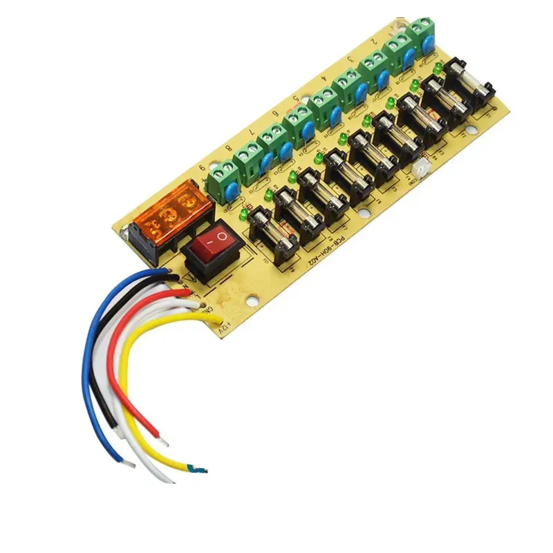
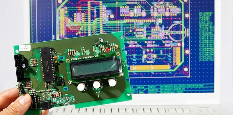
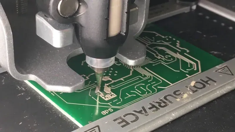
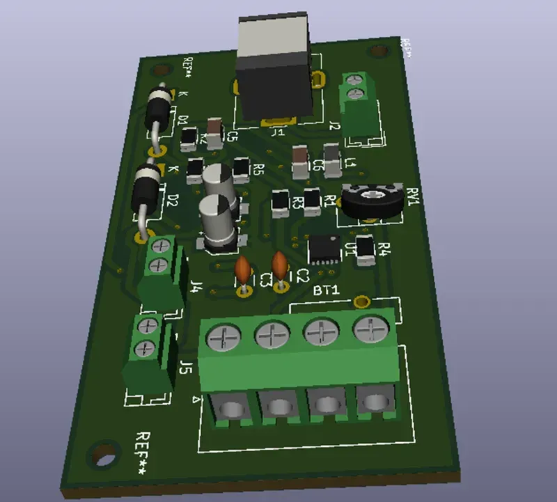
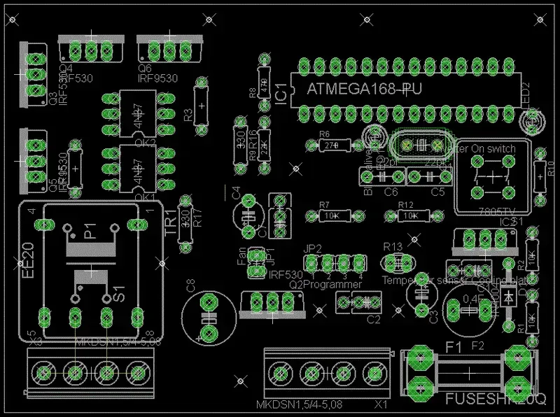
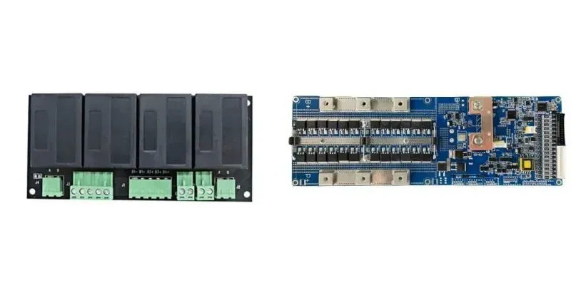
In an era defined by the urgent need for sustainable and accessible energy, distributed energy access (DEA) solutions are emerging as a pivotal force. These solutions, encompassing off-grid solar systems, microgrids, and renewable energy storage, hold the key to unlocking energy access for remote communities and underserved populations. At the heart of these innovative systems lies the printed circuit board (PCB), the unsung hero enabling efficient power management, control, and distribution. Zero One Solution Limited, with its rapid prototyping and manufacturing expertise, is committed to providing high-quality PCB solutions that empower DEA initiatives globally. Let’s explore how our advanced PCB solutions are driving the distributed energy revolution, transforming lives and building a more sustainable future.
The Critical Role of PCBs in Distributed Energy Access
Distributed Energy PCB Board
Printed Circuit Boards (PCBs) are the indispensable foundation upon which modern distributed energy access (DEA) systems are built. Far from being mere connectors, PCBs serve as the intelligent backbone, orchestrating the complex interplay of power generation, conversion, storage, and distribution. Their critical role lies in enabling the high efficiency, robust control, and seamless integration required for reliable and sustainable energy access, particularly in off-grid or remote applications where consistent power is paramount. Without advanced PCB technology, the decentralized, resilient nature of DEA solutions would be fundamentally unachievable, making them central to global efforts in energy equity and decarbonization.
Efficient Power Conversion PCBs facilitate the integration of power converters (AC/DC, DC/DC) essential for transforming raw energy inputs (e.g., solar DC) into usable electricity, minimizing losses and optimizing energy harvest. High-frequency designs and advanced material selection are crucial for maximizing conversion efficiency and thermal management in these critical stages, directly impacting system performance and longevity. Industry data indicates that optimized PCB layouts can reduce power conversion losses by up to 5% compared to sub-optimal designs, translating to significant energy savings over a system's lifespan, especially in low-power distributed networks. (Source: IEEE Journal of Power Electronics)
Precise Control and Management They host microcontrollers and communication interfaces that monitor system parameters, manage battery charging/discharging cycles, and control power flow, ensuring stable and safe operation. The precision of PCB trace routing and component placement directly impacts signal integrity, which is vital for accurate data acquisition and responsive control algorithms. For example, in smart microgrids, PCBs enable real-time load balancing and fault detection through embedded control logic, preventing outages and enhancing grid stability. Research from the Fraunhofer Institute for Solar Energy Systems highlights the role of integrated PCB-based control units in achieving over 98% operational reliability in decentralized photovoltaic systems.
Key Function
PCB Contribution
Impact on DEA System
Energy Harvesting
Integrates MPPT controllers and power optimizers
Maximizes energy capture from variable sources (solar, wind)
Power Storage
Manages Battery Management Systems (BMS)
Ensures battery longevity, safety, and efficient charge/discharge
Power Distribution
Routes power efficiently to loads, manages load balancing
Provides stable and reliable power delivery to end-users
System Monitoring & Control
Hosts sensors, microcontrollers, communication modules
Enables remote monitoring, diagnostics, and intelligent grid management
Challenges in Designing PCBs for Harsh Environments
PCB Board in Extreme Temperatures
Designing Printed Circuit Boards (PCBs) for distributed energy access (DEA) systems presents unique and demanding challenges, primarily due to their operation in often harsh and unpredictable environments. Unlike consumer electronics, DEA PCBs must maintain robust functionality under extreme temperatures, high humidity, significant vibrations, and potential chemical exposure, directly impacting system reliability and longevity. Addressing these environmental stressors through meticulous material selection, advanced thermal management, and robust mechanical design is paramount to ensuring the uninterrupted performance of critical energy infrastructure.
Environmental Factor
Typical Impact on PCBs
Design Considerations by Zero One Solution Limited
Extreme Temperatures
Material degradation, component failure, thermal cycling fatigue
High Tg laminates, optimized thermal vias, heat sinks, active cooling strategies, component derating for extended temperature ranges.
][
]
Zero One Solution
+ [Meaning of The Text Description](#man--data-security-system-design-for-public and commercial building, including security control system).{
PCB Rapid Prototyping
Zero One Solution Limited has established itself as a leader in providing cutting-edge PCB solutions specifically designed for the distributed energy access (DEA) sector. Our expertise stems from a deep understanding of the unique challenges and demands of these critical applications, allowing us to deliver robust, reliable, and high-performance PCBs that underpin the stability and efficiency of modern energy infrastructure. Our commitment to rapid prototyping and advanced manufacturing capabilities ensures that clients can bring their innovative energy solutions to market faster and with greater confidence.
What makes Zero One Solution's PCB solutions ideal for Distributed Energy Access (DEA) applications? Our solutions are engineered for resilience and efficiency, crucial for DEA systems often operating in harsh, remote, or off-grid environments. We leverage advanced materials, precise design methodologies, and robust manufacturing processes to ensure our PCBs withstand extreme temperatures, humidity, vibrations, and other environmental stressors. Furthermore, our focus on rapid prototyping significantly accelerates the development cycle for new DEA products, allowing for quick iterations and market entry.
How does Zero One Solution address the need for rapid prototyping in the DEA sector? Rapid prototyping is a cornerstone of our service offering. We understand the critical need for speed in the rapidly evolving DEA market. Our streamlined design-to-manufacturing process, coupled with state-of-the-art equipment and agile methodologies, enables us to produce high-quality prototypes in significantly reduced timeframes. This empowers our clients to quickly test, validate, and refine their designs, accelerating their product development and deployment cycles.
What are the key quality control measures in place for DEA PCB manufacturing at Zero One Solution? Quality is paramount in DEA applications where reliability directly impacts energy access. We implement a multi-stage quality control process, from meticulous component sourcing and material inspection to in-process testing and final functional verification. Our manufacturing facilities adhere to stringent industry standards (e.g., ISO 9001, IPC standards), and we employ advanced testing methodologies like Automated Optical Inspection (AOI) and X-ray inspection to ensure every PCB meets the highest performance and reliability benchmarks.
Can Zero One Solution's PCBs integrate with various distributed energy technologies? Yes, our expertise extends across the diverse landscape of distributed energy technologies. We design and manufacture PCBs for a wide range of applications, including solar photovoltaic systems, wind energy converters, battery energy storage systems (BESS), microgrids, and off-grid power solutions. Our designs are flexible and adaptable, capable of accommodating various power management, control, and communication protocols specific to each technology.
How does Zero One Solution ensure the long-term reliability and durability of PCBs in DEA environments? Ensuring long-term reliability is central to our design philosophy. We meticulously select components and materials that exhibit exceptional durability and performance under challenging conditions. Our design processes incorporate robust thermal management solutions, impedance control, and EMI/EMC considerations to prevent premature failure. Furthermore, we emphasize conformal coating and ruggedized enclosures where necessary to provide additional protection against environmental factors, extending the operational lifespan of the PCBs.
Our Comprehensive PCB Services for DEA Projects
At Zero One Solution, we recognize the intricate demands of Distributed Energy Access (DEA) projects, which necessitate more than just component supply
—they require an integrated, end-to-end PCB solution that covers every stage from conceptualization to final assembly. Our comprehensive suite of services is meticulously designed to streamline your DEA project development, ensuring optimal performance, reliability, and expedited market entry for critical energy infrastructure.
PCB Design and Layout for DEA Our expert engineers provide advanced PCB design and layout services specifically optimized for distributed energy systems, focusing on power efficiency, signal integrity, thermal management, and robust performance in varied environmental conditions. We utilize cutting-edge CAD tools to deliver designs that meet stringent industry standards and project specifications.
Rapid Prototyping and Iteration Leveraging our core strength in rapid prototyping, we accelerate your development cycle for DEA boards. Quick-turn prototypes allow for swift testing, validation, and design iteration, significantly reducing time-to-market and enabling agile adjustments to complex energy system requirements.
High-Volume PCB Manufacturing From small batches to large-scale production, our state-of-the-art manufacturing facilities in Shenzhen are equipped to handle diverse production volumes for DEA PCBs. We adhere to strict quality control protocols, ensuring every board meets the highest standards of durability and functionality essential for long-term distributed energy applications.
Advanced PCB Assembly (PCBA) Our comprehensive PCBA services include Surface Mount Technology (SMT), Through-Hole Technology (THT), and mixed-technology assembly. We specialize in assembling complex DEA boards with high precision, including integration of power management ICs, communication modules, and sensing components, ensuring seamless functionality.
Rigorous Quality Assurance and Testing Quality is paramount in DEA solutions. We implement multi-stage testing protocols, including AOI (Automated Optical Inspection), X-ray inspection, ICT (In-Circuit Test), and functional testing, to guarantee the reliability and performance of every PCB. Our commitment to quality minimizes field failures and maximizes system uptime in distributed energy networks.
Service Aspect
Zero One Solution Advantage
Impact on DEA Projects
Design for Manufacturability (DFM)
Early DFM analysis by our engineers
Reduces manufacturing costs, improves yield, accelerates production for DEA boards
Component Sourcing & Management
Global network for high-quality, reliable components
Ensures supply chain stability, reduces lead times, critical for timely DEA deployments
Conformal Coating & Potting
Expert application for environmental protection
Enhances PCB durability in harsh DEA environments, extends lifespan
Post-Assembly Rework & Repair
Skilled technicians for component replacement/repair
Minimizes waste, extends product life, supports sustainability in DEA applications
PCB Design Considerations for Solar Power Systems
Solar Power PCB Board
Designing Printed Circuit Boards (PCBs) for solar power systems necessitates a meticulous approach to ensure optimal performance, longevity, and efficiency. These systems, ranging from small-scale residential setups to large utility-scale solar farms, demand PCBs that can reliably handle high power conversion, integrate Maximum Power Point Tracking (MPPT) efficiently, and manage thermal dissipation effectively under varying environmental conditions. The core challenge lies in balancing electrical integrity with physical durability to maximize energy harvesting from solar arrays.
What are the critical PCB design aspects for efficient solar power conversion? Efficient solar power conversion in PCBs relies heavily on robust power path design, minimal trace inductance, and low-resistance copper pours. High-frequency switching components, such as those found in DC-DC converters, require careful layout to reduce EMI and optimize power transfer. Utilizing appropriate component selection with low ESR/ESL and high current ratings is also paramount to minimize losses and ensure stable operation. Furthermore, the strategic placement of decoupling capacitors close to switching nodes helps in filtering noise and maintaining stable voltage levels.
How does MPPT integration impact PCB design for solar systems? MPPT (Maximum Power Point Tracking) integration significantly influences PCB design by requiring dedicated control circuitry and accurate sensing capabilities. The PCB must accommodate current and voltage sensors, analog-to-digital converters (ADCs), and microcontrollers or DSPs that execute complex MPPT algorithms. Signal integrity becomes crucial to ensure precise readings for the MPPT algorithm to accurately determine and track the solar panel's maximum power point. This often involves careful routing to prevent noise coupling and ensure signal fidelity for optimal energy yield.
What are the key thermal management strategies for solar power system PCBs? Thermal management in solar power system PCBs is critical due to the heat generated by power electronics and exposure to external environmental heat. Key strategies include using thicker copper layers for better heat spreading, incorporating thermal vias to transfer heat to ground planes or heatsinks, and optimizing component placement to avoid hot spots. Utilizing thermally conductive substrates or external heatsinks for high-power components like MOSFETs and IGBTs is also essential. Advanced thermal simulation during the design phase helps predict and mitigate potential thermal issues, ensuring component reliability and system longevity.
What materials are recommended for solar PCB substrates to withstand outdoor conditions? For solar PCB substrates exposed to outdoor conditions, materials with excellent thermal stability, moisture resistance, and UV resistance are recommended. FR-4 is a common choice, but for harsher environments, materials like high-Tg (glass transition temperature) FR-4 or even specialized ceramic-based substrates offer superior performance. Polyimide or flexible PCBs might be considered for specific applications requiring flexibility or conformability. The choice also depends on the required dielectric strength and insulation properties to prevent electrical breakdown in high-voltage solar arrays.
How does Zero One Solution address reliability and durability in solar PCB designs? Zero One Solution addresses reliability and durability in solar PCB designs through a multi-faceted approach. We employ advanced simulation tools for thermal and electrical analysis, ensuring optimal performance under various load and environmental conditions. Our material selection prioritizes high-grade, durable substrates and components capable of withstanding extreme temperatures, humidity, and UV exposure. Furthermore, our rapid prototyping and rigorous testing procedures, including accelerated life testing and environmental stress screening, validate the design's robustness before mass production, guaranteeing long-term reliability for solar power applications.
PCB Solutions for Microgrids: Ensuring Stability and Reliability
Microgrid PCB Board
Printed Circuit Boards (PCBs) are the foundational technology underpinning the stability and reliability of microgrids, serving as the intelligent backbone for managing decentralized energy generation, storage, and consumption. Their precise design and robust construction are critical for orchestrating complex functions such as seamless grid synchronization, dynamic load balancing, and efficient communication protocols, thereby ensuring uninterrupted and dependable power distribution in both grid-connected and islanded modes.
What specific challenges do PCBs address in microgrid stability? PCBs in microgrids address critical challenges like voltage and frequency stabilization, power flow control, fault detection and isolation, and protection against overcurrents and short circuits. They facilitate the precise synchronization of distributed energy resources (DERs) with the main grid or within the microgrid itself, preventing oscillations and ensuring stable power delivery.
How do PCBs enable effective grid synchronization in microgrids? PCBs enable effective grid synchronization through integrated control circuitry that precisely monitors voltage, frequency, and phase angle. They incorporate sophisticated digital signal processors (DSPs) and microcontrollers to execute advanced algorithms for phase-locked loops (PLLs), ensuring that DERs connect and disconnect from the grid or other microgrid components smoothly, minimizing transients and maintaining power quality.
What role do PCBs play in load balancing within microgrids? PCBs are instrumental in dynamic load balancing within microgrids by integrating real-time data acquisition and intelligent control mechanisms. They monitor energy generation and consumption across the microgrid, enabling rapid adjustments to power output from DERs and intelligent shedding or restoration of non-critical loads. This ensures that demand is continuously met by available supply, optimizing energy utilization and preventing system overload or undervoltage conditions.
How do communication protocols on PCBs contribute to microgrid reliability? Communication protocols on PCBs are vital for microgrid reliability by facilitating seamless data exchange between all components, including DERs, energy storage systems, loads, and the central microgrid controller. Protocols like Modbus, DNP3, and IEC 61850 are implemented on PCBs to enable real-time monitoring, fault diagnostics, and rapid command execution, ensuring coordinated operation and swift response to changing conditions, thereby enhancing overall system resilience.
What are the key design considerations for microgrid PCBs to ensure long-term reliability? Key design considerations for microgrid PCBs to ensure long-term reliability include selecting robust materials resistant to environmental stressors (e.g., temperature extremes, humidity), incorporating effective thermal management solutions, designing for electromagnetic compatibility (EMC) to prevent interference, and implementing redundant pathways or fail-safe mechanisms for critical functions. High-quality components and rigorous testing protocols during manufacturing are also paramount to withstand continuous operation in dynamic microgrid environments.
Energy Storage PCB Solutions: Optimizing Battery Management
Energy Storage Battery Management PCB
Effective energy storage is paramount for the stability and efficiency of distributed energy systems, and at its core lies sophisticated Battery Management System (BMS) PCBs. These specialized boards are engineered to meticulously monitor, control, and protect battery packs, ensuring optimal performance, extended lifespan, and paramount safety in dynamic energy environments.
What are the primary functions of PCBs in energy storage systems? PCBs in energy storage systems primarily manage battery charging and discharging, monitor individual cell voltage and temperature, balance cell states, and provide critical safety functions like overcurrent, overvoltage, undervoltage, and thermal protection. They are the central nervous system for battery packs, optimizing their performance and longevity.
What are the key design challenges for energy storage PCB solutions? Key design challenges for energy storage PCBs include managing high current densities to prevent thermal runaway, ensuring robust electromagnetic compatibility (EMC) in noisy environments, achieving high precision in voltage and current sensing for accurate battery state estimation, and designing for compact form factors while maintaining effective heat dissipation. Reliability under various environmental conditions is also crucial.
How do PCBs contribute to battery safety in energy storage applications? PCBs contribute significantly to battery safety by integrating protective circuits that prevent overcharging, over-discharging, short circuits, and extreme temperatures. They enable real-time fault detection and isolation, allowing the system to safely shut down or isolate problematic cells, thereby mitigating risks of fire or explosion and ensuring compliance with safety standards like UL 1973 or IEC 62619.
What role does thermal management play in Energy Storage PCB Solutions? Thermal management is critical in energy storage PCBs to prevent overheating, which can degrade battery performance, shorten lifespan, and pose safety risks. PCBs are designed with features like optimized copper pour, thermal vias, and strategic component placement to dissipate heat efficiently. Advanced designs may incorporate integrated heat sinks or liquid cooling interfaces to maintain optimal operating temperatures for high-power battery packs.
Why is cell balancing important, and how do PCBs facilitate it? Cell balancing is vital to ensure all cells within a battery pack discharge and charge uniformly, maximizing the pack's usable capacity and extending its overall lifespan. PCBs facilitate cell balancing through active or passive balancing circuits. Passive balancing dissipates excess energy from higher-voltage cells, while active balancing transfers energy between cells, both managed by the BMS on the PCB to maintain cell voltage equilibrium.
Case Studies: Zero One Solution
The most prominent characteristic of distributed energy access is decentralized management, which allows resources to be managed locally, improving system resilience and reducing overall infrastructure costs while enabling effective integration of diverse renewable energy sources. This fundamental difference from traditional centralized grids necessitates specialized Printed Circuit Board (PCB) solutions to manage power flow, control, communication, and system stability at the local level. These tailored PCBs are critical for the efficiency, reliability, and security of distributed energy systems, facilitating everything from intelligent device control to seamless grid interaction.Zero One Solution Limited has a proven track record of delivering successful Distributed Energy Access (DEA) projects, providing high-quality, customized PCB solutions that address the unique challenges of decentralized energy systems. Our commitment to rapid prototyping and advanced manufacturing ensures that our clients receive robust and efficient PCBs, enabling faster product development and deployment of innovative energy solutions. We pride ourselves on empowering the global transition to sustainable and resilient energy infrastructure through our cutting-edge PCB technology.
Optimizing Solar Inverter Performance in Rural Communities Zero One Solution partnered with a non-profit organization to develop highly efficient PCB assemblies for off-grid solar inverters deployed in remote African villages. Our customized MPPT (Maximum Power Point Tracking) PCBs significantly improved energy harvesting from solar panels, increasing power output by an average of 15% and directly enhancing the availability of electricity for lighting, communication, and essential services. The robust design ensured reliable operation despite extreme temperature fluctuations and dust, demonstrating our ability to deliver durable solutions for challenging environments.
Enhancing Microgrid Stability for Island Nations In a project aimed at providing stable power to a small island nation heavily reliant on diesel generators, Zero One Solution engineered advanced PCBs for a hybrid microgrid system integrating solar, wind, and battery storage. Our PCBs for grid synchronization and load balancing allowed for seamless transition between energy sources and optimized power distribution, reducing reliance on fossil fuels by 30% and significantly decreasing energy costs. The precision and reliability of our PCB solutions were crucial in maintaining grid stability and ensuring uninterrupted power supply.
Advanced Battery Management for Urban Energy Storage For a commercial energy storage project in a densely populated urban area, Zero One Solution developed sophisticated Battery Management System (BMS) PCBs. These boards incorporated advanced algorithms for charge and discharge control, cell balancing, and comprehensive safety features, extending battery lifespan by 25% and preventing critical failures. Our rapid prototyping capabilities enabled quick iterations and optimization, delivering a compact and highly efficient BMS solution that met stringent urban regulatory and space requirements.
Smart Metering Integration for Community Grids Zero One Solution collaborated on a smart metering initiative for a community-owned distributed grid in Southeast Asia. We designed and manufactured compact, low-power PCBs for smart meters that enabled real-time energy monitoring, consumption analysis, and remote control. Our PCBs facilitated seamless communication between meters and the central grid management system, leading to a 20% improvement in energy efficiency and empowering residents with better control over their energy usage, while ensuring data integrity and security in a dynamic distributed network.
Partnering with Zero One Solution: Benefits and Advantages
Choosing the right PCB partner is paramount for the success of Distributed Energy Access (DEA) projects, which demand precision, reliability, and speed. Zero One Solution Limited stands as a premier choice, offering a unique blend of rapid prototyping, high-quality manufacturing, and unparalleled expert support. Our strategic location in Shenzhen, coupled with a global supply chain, ensures that we are not just a supplier, but a critical extension of your R&D and production teams, enabling faster time-to-market and superior product performance in the dynamic distributed energy sector.
Rapid Prototyping & Agile Development Zero One Solution excels in rapid-response R&D prototype manufacturing, significantly reducing development cycles. This agility allows for quick iteration and validation of designs, which is crucial for innovative DEA solutions where speed to market is a competitive advantage. Our streamlined processes mean your conceptual designs quickly transform into functional prototypes.
Uncompromising Quality & Reliability With over a decade of expertise, Zero One Solution adheres to rigorous quality control standards throughout the PCB design, manufacturing, and assembly processes. Our commitment to high-quality output ensures that the PCBs for your distributed energy access systems are robust, reliable, and capable of performing optimally in diverse and often harsh environmental conditions, minimizing field failures and maintenance costs.
End-to-End, One-Stop PCB Solutions We offer a comprehensive suite of services, from initial PCB design and engineering support to manufacturing and final assembly. This integrated approach simplifies your supply chain, reduces coordination complexities, and ensures seamless transitions between project phases, providing you with a single point of contact for all your PCB needs in DEA projects.
Expert Technical Support & Collaborative Partnership Our team comprises veteran engineers with extensive experience in PCB solutions, particularly for complex applications like distributed energy. We provide dedicated technical support, collaborating closely with your team to overcome design challenges, optimize performance, and ensure that your DEA board solutions are not only technically sound but also cost-effective and scalable.
Strategic Global Reach & Supply Chain Efficiency Headquartered in Shenzhen and with a branch in Dubai, Zero One Solution leverages a robust global PCBA supply chain network. This strategic positioning provides unparalleled access to a wide range of components and materials, enabling efficient procurement, reducing lead times, and ensuring competitive pricing, ultimately benefiting your project's budget and timeline.
In conclusion, Distributed Energy Access (DEA) solutions are crucial for sustainable development, and reliable PCBs are at their core. Zero One Solution Limited is dedicated to providing cutting-edge PCB solutions that drive DEA initiatives, offering expertise in rapid prototyping, manufacturing, and assembly. By partnering with us, you gain access to high-quality, innovative PCBs that empower communities, improve energy access, and contribute to a greener future. Contact Zero One Solution Limited today to learn more about how our PCB solutions can power your next distributed energy project and transform the lives of those in need. Let's collaborate to build a sustainable and energy-accessible world for everyone.