
As automotive electronic systems become increasingly complex, the push for miniaturization is no longer a luxury—it is a necessity. To maintain a competitive edge, Tier-1 suppliers are turning to High-Density Interconnect (HDI) technology to shrink footprints without sacrificing performance. This guide explores the strategic transition to HDI and how it redefines manufacturing efficiency.
The Evolution of Automotive Electronics and the HDI Imperative
The Shift Toward Complexity
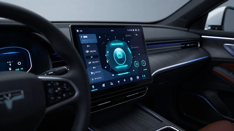
As modern vehicles transition into software-defined platforms, traditional Printed Circuit Board (PCB) design methods have reached their physical limits. The integration of advanced infotainment systems, high-resolution cockpit displays, and safety-critical ADAS modules requires significantly higher data throughput and miniaturization. HDI technology serves as the architectural bridge, allowing for thinner traces, smaller vias, and increased component density, which directly addresses the footprint constraints of current automotive dashboards.
Traditional PCB vs. HDI Architecture
| Feature | Traditional PCB | HDI PCB |
|---|---|---|
| Via Technology | Through-hole | Micro-via (Laser-drilled) |
| Trace Width | Standard (>= 100µm) | Fine (<= 50µm) |
| Routing Density | Low | High |
| Signal Integrity | Moderate | Superior |
Optimizing ROI Through HDI
Transitioning to HDI is not merely a technical upgrade; it is a financial strategy. By utilizing micro-vias and sequential lamination, manufacturers can significantly reduce the total layer count and board size. Smaller, more efficient PCBs require less base material and reduce the overall weight of the vehicle, contributing to improved fuel efficiency and lower logistics costs over the production lifecycle.
Frequently Asked Questions
- Why is HDI necessary for modern infotainment?
Modern infotainment requires high-speed data buses and complex processors that demand shorter signal paths to minimize latency and electromagnetic interference, which HDI uniquely provides. - Does HDI increase unit production costs?
While the per-unit fabrication cost of HDI may be higher than traditional boards, the reduction in PCB size and potential for multi-function integration often yields a lower total cost of ownership at the system level. - How does HDI impact reliability?
HDI allows for reduced thermal strain and improved signal integrity, which are critical for meeting the stringent vibration and temperature standards defined by automotive AEC-Q standards.
Understanding HDI: Microvias and Buried Traces
The Mechanics of Microvias and Buried Traces
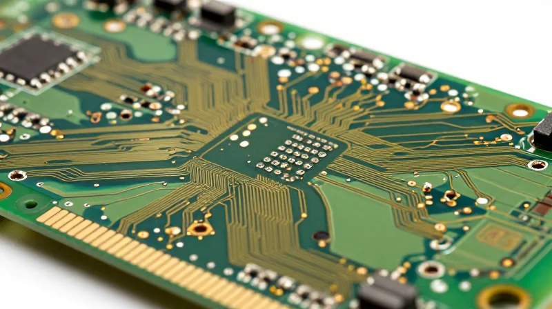
HDI technology shifts the paradigm from traditional through-hole via designs to a more agile stack-up utilizing laser-drilled microvias. By minimizing the physical footprint of interconnects, HDI allows for higher routing density in tighter spaces, which is critical for the compact form factors required in modern automotive cockpit controllers.
| Feature | Traditional PCB | HDI Architecture |
|---|---|---|
| Via Type | Through-hole | Microvia/Blind/Buried |
| Routing Density | Low to Moderate | High |
| Signal Integrity | Lower (Stub interference) | Superior (Reduced parasitic inductance) |
| Layer Count | Higher/Bulkier | Optimized/Compact |
Optimizing Signal Integrity through Advanced Routing
In high-speed infotainment applications, signal integrity is paramount. Through-hole vias often act as 'stubs' that cause reflections and resonance, degrading performance. Microvias, by design, connect only the necessary layers, effectively eliminating these stubs. Furthermore, buried vias allow for signal routing in internal layers, shielding sensitive signals from electromagnetic interference (EMI) and improving the overall system reliability.
Frequently Asked Questions
- Why do microvias improve ROI?
By allowing higher density, you can reduce the total layer count or the board's physical size, directly lowering material costs and assembly complexity for infotainment units. - How do buried vias affect thermal management?
While they increase density, buried vias are strategically placed to enable optimized ground plane connectivity, facilitating better heat dissipation throughout the PCB stack. - Are microvias reliable for automotive vibration?
Yes, laser-drilled microvias provide a more robust structural connection than standard vias, especially when paired with sequential lamination processes designed for extreme automotive environments.
Reducing Board Footprint: Maximizing Space in Tight Cockpits
The Challenge of Compact Automotive Environments
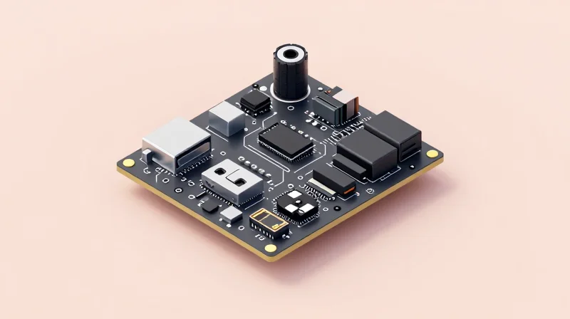
Modern automotive cockpits are shifting toward integrated, screen-heavy dashboard architectures that leave minimal physical space for control electronics. Traditional multilayer PCBs, burdened by large via structures and sprawling trace patterns, often exceed the physical footprint requirements for these modular units. HDI PCB architecture mitigates this by utilizing thinner laminates and high-density routing, enabling a smaller overall board size without sacrificing functionality.
HDI vs. Traditional PCB Footprint Comparison
| Feature | Traditional PCB | HDI Architecture |
|---|---|---|
| Via Diameter | 0.2mm - 0.3mm | <0.1mm (Microvia) |
| Layer Count | High (to manage routing) | Low (higher density per layer) |
| Component Density | Moderate | Very High |
| Board Size | Larger | Reduced by 30-50% |
Space Optimization Strategies
By shifting to microvia technology, designers can implement 'via-in-pad' designs, which move connections directly under surface-mount devices. This eliminates the need for external escape routing patterns that consume valuable surface area. The cumulative effect is a leaner, lighter electronic module that fits into slimmer dashboard housings, providing greater design flexibility for aesthetics and cabin ergonomics.
Frequently Asked Questions
- How does reducing board size impact ROI?
Smaller boards require less raw laminate material and enable smaller mechanical housing enclosures, which lowers overall manufacturing and logistics costs. - Does higher density increase thermal risk?
While component proximity increases, HDI allows for optimized thermal via placement, enabling more efficient heat dissipation directly from the component to inner copper planes. - Can HDI accommodate complex infotainment SoCs?
Yes, the fine-pitch routing capabilities of HDI are specifically designed to handle the high-pin-count BGA packages typical of modern automotive processors.
Case Study: Achieving ROI Through Component Count Reduction
The Challenge: Balancing High Performance and Cost
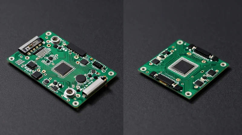
An automotive Tier-1 supplier recently faced a critical hurdle: their next-generation infotainment head unit required advanced processing capabilities that were straining the physical limits of traditional 12-layer through-hole PCB technology. The initial design suffered from high signal integrity issues and a bulky footprint that compromised internal vehicle ergonomics, leading to ballooning assembly costs.
Architectural Shift: Transitioning to HDI
By migrating to a 1-n-1 HDI stackup, the engineering team replaced standard through-hole vias with laser-drilled microvias. This architectural shift allowed for increased routing density on inner layers, effectively consolidating two signal layers and reducing the board from 12 layers down to 8. This reduction did more than shrink the form factor; it directly impacted the bottom line by simplifying the fabrication process and increasing manufacturing throughput.
| Metric | Traditional PCB | HDI Optimized PCB |
|---|---|---|
| Layer Count | 12 Layers | 8 Layers |
| Via Technology | Through-hole | Microvia (Laser) |
| BOM Complexity | High | Low |
| PCB Unit Cost | Baseline | -18% reduction |
Quantifiable ROI Results
The transition yielded three primary ROI drivers. First, the reduced layer count directly lowered raw material and lamination costs. Second, the optimized trace routing improved signal integrity, eliminating the need for expensive high-frequency shielding components. Finally, the compact footprint enabled a smaller, lower-cost housing enclosure for the final infotainment assembly.
Frequently Asked Questions
- Does the higher per-unit cost of HDI laser drilling hurt ROI?
While microvia fabrication has a higher upfront technical cost, the total BOM savings derived from reducing the total number of PCB layers significantly outweighs these costs at high production volumes. - How does component count reduction affect long-term reliability?
By consolidating functionality into fewer layers, you reduce the number of potential solder joint failures and interconnections, leading to a more robust final assembly and lower warranty costs. - Is the transition to HDI suitable for all automotive infotainment projects?
It is most effective for complex systems requiring high-speed data processing; for simpler, low-I/O applications, traditional multi-layer designs may still provide a more cost-effective baseline.
Accelerating Time-to-Market for Tier-1 Suppliers
Streamlining the Prototype-to-Production Lifecycle
For Tier-1 suppliers, the transition from prototype to mass production is often fraught with re-spins and yield volatility. HDI technology shifts the paradigm by enabling higher component density on a single layer, which reduces the need for complex multi-board assemblies and decreases the number of mechanical interfaces. By consolidating functionality into a smaller, more efficient board architecture, engineers can validate designs faster, as the reduction in physical board size directly correlates with fewer signal integrity issues and shorter trace lengths that require complex simulation.
| Phase | Traditional PCB Approach | HDI-Ready Architecture |
|---|---|---|
| Design Validation | Multiple iterations due to signal noise | Faster cycles via high-density signal paths |
| Component Sourcing | Complex multi-board BOM management | Streamlined BOM via high-density integration |
| Manufacturing | High risk of assembly alignment errors | Automated microvia precision ensures high yield |
Common Questions on HDI Implementation
- How does HDI reduce manufacturing complexity?
HDI allows for the use of microvias and build-up processes that eliminate the need for traditional through-hole drilling, reducing the physical complexity and potential failure points during assembly. - Does HDI accelerate time-to-market despite higher PCB unit costs?
Yes. While the PCB unit cost may be higher, the overall system cost is lower due to reduced assembly time, fewer materials, and accelerated testing phases that decrease the total time to market. - Is HDI reliable enough for automotive-grade infotainment?
Modern laser-drilling and plating technologies have made HDI highly reliable for the automotive sector, provided that the stack-up design accounts for coefficient of thermal expansion (CTE) matching.
Ultimately, Tier-1 suppliers who prioritize HDI architecture gain a competitive edge by lowering the cost of failure. By minimizing physical board dimensions, these designs facilitate easier enclosure integration, allowing for modular updates to infotainment systems without necessitating complete chassis or PCB redesigns.
Thermal Management and Reliability in HDI Designs
Managing Thermal Density in Compact Architectures
As HDI technology compresses more functionality into smaller footprints, power density increases, creating significant thermal challenges. Unlike traditional multilayer boards, HDI designs rely heavily on microvias and specialized copper-filled structures to act as thermal conduits, channeling heat away from high-performance SoC processors and toward the heat sink or chassis. Engineers must implement optimized copper pouring and thermal relief patterns to prevent localized hotspots that degrade sensitive IC performance.
| Thermal Strategy | Implementation Method | Performance Impact |
|---|---|---|
| Thermal Vias | Copper-filled microvias in thermal pads | Direct heat path to inner layers |
| Copper Weight | Increased inner-layer copper thickness | Improved lateral heat spreading |
| Thermal Interface | High-conductivity TIM placement | Lower junction-to-ambient resistance |
Ensuring Reliability through Automotive Standards
Automotive infotainment systems operate under extreme environmental conditions, from sub-zero starts to cabin temperatures exceeding 85°C. Reliability in HDI designs is governed by strict adherence to IPC-6012 automotive addendums and AEC-Q100 standards. Ensuring solder joint integrity and preventing microvia fatigue during repeated thermal cycling are the primary focus areas for Tier-1 suppliers seeking long-term field reliability.
- How do microvias handle thermal stress?
Microvias, specifically stacked or staggered configurations, are designed to withstand high coefficient of thermal expansion (CTE) mismatches through precisely controlled aspect ratios and copper plating processes. - Why is thermal simulation vital for HDI?
Thermal modeling during the design phase identifies heat concentration areas, allowing for layout adjustments before physical prototyping, which significantly reduces development costs. - What testing protocols are standard for automotive HDI?
Boards undergo rigorous Highly Accelerated Life Testing (HALT) and thermal shock testing to replicate ten years of vehicle operation under harsh environmental stressors.
Strategic Cost Analysis: Long-term Savings vs. Initial Complexity

While HDI technology requires a higher initial investment in design complexity and advanced fabrication, these costs are systematically offset by reduced layer counts, smaller footprints, and improved production yields. The strategic transition to HDI is not merely a performance upgrade but a financial lever that compresses product life-cycle costs by mitigating expensive material waste and streamlining final assembly processes.
Comparative Cost Dynamics: HDI vs. Conventional Multilayer
| Cost Factor | Conventional PCB | HDI PCB Architecture |
|---|---|---|
| Design Complexity | Low - Standard Routing | High - Microvia Optimization |
| Component Count | High - Larger Footprint | Lower - Integrated Functionality |
| Assembly Throughput | Moderate - Multi-pass | High - Streamlined SMT |
| Field Failure Rate | Higher due to Bulk | Lower due to Signal Integrity |
Evaluating the Long-Term ROI
The primary barrier to HDI adoption is often perceived as the 'complexity tax'—the engineering hours required for high-density routing and the higher cost per board of HDI fabrication. However, when evaluating the total cost of ownership for a Tier-1 automotive platform, the ROI becomes clear through secondary cost savings:
- Material Conservation
HDI allows for smaller form factors, significantly reducing the board area and reducing overall substrate material costs across high-volume production runs. - Operational Reliability
By consolidating signal paths and reducing electrical noise, HDI decreases the incidence of field-return claims, saving millions in warranty and support costs. - Platform Scalability
The standardized microvia structures facilitate faster board iterations, allowing manufacturers to reuse core HDI designs across multiple infotainment tiers.
Strategic Considerations for OEMs
Transitioning to an HDI-centric roadmap requires a shift from viewing PCBs as commodity components to viewing them as critical intellectual property. Organizations that front-load the design process with rigorous HDI simulation and simulation-driven layout practices inherently reduce the risks of costly design spins late in the validation phase, thereby securing a definitive competitive advantage in the high-performance infotainment market.
Best Practices for Implementing HDI in Automotive Projects
The successful integration of High-Density Interconnect (HDI) PCBs in automotive infotainment systems necessitates a departure from legacy design methodologies. To maximize Return on Investment (ROI), engineering teams must prioritize front-end design integrity, select materials optimized for thermal stability, and foster deep technical partnerships with fabricators from the project's inception.
Design Rule Checks (DRC) for HDI Success
Automotive infotainment systems push the boundaries of signal integrity and packaging density. Designers must establish stringent DRC parameters that account for the unique manufacturing constraints of micro-vias and high-layer counts.
- Automated DRC Setup
Utilize constraint-driven design software to flag potential violations in pad-to-trace spacing and via-in-pad transitions automatically, reducing human error in complex dense routing. - Signal Integrity (SI) Verification
Implement pre-layout simulation to address high-speed data path concerns early, minimizing costly re-spins caused by EMI/EMC failures in complex infotainment architectures. - Stack-up Symmetry
Ensure balanced copper distribution across layers to prevent board warpage during the reflow process, a critical factor for maintaining long-term reliability in vehicle environments.
Material Selection and Fabrication Synergy
Selecting the right laminate materials and working closely with your fabricator are the primary determinants of yield rates. Automotive-grade HDI boards require materials that withstand high thermal cycling without compromising electrical performance.
| Parameter | Standard PCB | Automotive HDI |
|---|---|---|
| Glass Transition (Tg) | 130-150°C | >170°C |
| CTE Control | Variable | Minimized Z-axis expansion |
| Signal Loss | Standard Loss | Low or Ultra-Low Loss |
Best Practices for Fabricator Collaboration
- Early Involvement (DFM/DFA)
Engage your PCB manufacturer before finalizing board dimensions; their insights on panel utilization can significantly reduce material waste and manufacturing costs. - Process Capabilities Alignment
Review your design against the manufacturer's specific laser-drilling and plating tolerances to ensure high yields and minimize defect rates during mass production. - Quality Certification Verification
Confirm compliance with IATF 16949 standards for every layer of the manufacturing process to guarantee the automotive safety and longevity required by OEM partners.
By adopting HDI technology, automotive suppliers can effectively bridge the gap between aggressive miniaturization goals and bottom-line profitability. While the design complexity increases, the long-term gains in footprint optimization and time-to-market make it an essential pivot for modern electronics. Ready to optimize your hardware architecture? Contact our engineering team today for a consultation on your next HDI project.
