
Modern automotive infotainment units demand unprecedented processing power within increasingly constrained physical envelopes. As data rates climb and thermal envelopes shrink, the margin for error in PCB design vanishes. This guide provides a veteran's perspective on mastering DFM rules to ensure your high-reliability hardware meets the rigorous demands of the automotive industry.
The Evolution of Automotive HDI Demands
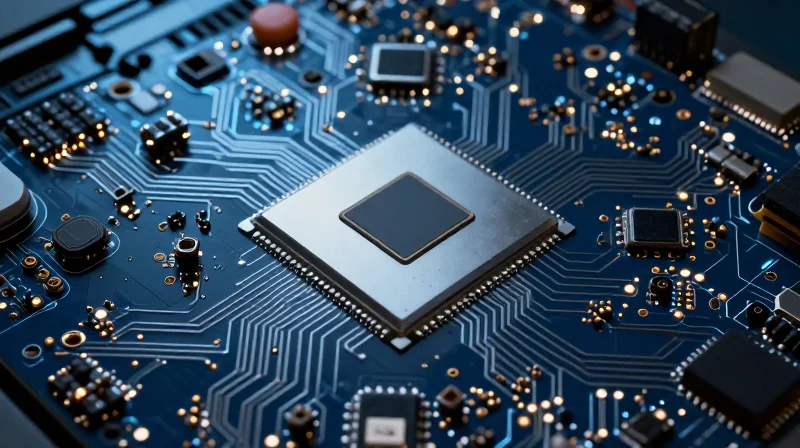
The Shift Toward HDI in Infotainment Systems
The automotive industry is experiencing a paradigm shift as infotainment units evolve from simple media players into powerful, AI-driven cockpit domain controllers. This transformation demands significantly higher component density and faster signal integrity. Traditional PCB manufacturing methods, which rely on through-hole vias and lower trace densities, are no longer sufficient to manage the complex routing required by modern high-pin-count SoCs (System-on-Chips) and high-speed memory interfaces like LPDDR5.
Comparative Analysis: Traditional PCB vs. HDI
| Feature | Traditional PCB | HDI PCB |
|---|---|---|
| Via Technology | Through-hole | Micro-via (Laser Drilled) |
| Routing Density | Low/Moderate | Very High |
| Trace/Space Width | Large (>100μm) | Fine (<50μm) |
| Performance | Limited Signal Integrity | High Signal/Power Integrity |
Key Drivers of HDI Adoption
- Miniaturization
Automotive electronic control units (ECUs) are shrinking to save weight and space, requiring more components to be packed into smaller footprints. - High-Speed Signal Integrity
HDI allows for shorter trace lengths and optimized return paths, critical for maintaining signal fidelity in high-frequency infotainment displays and telematics. - Thermal Management
Advanced HDI structures facilitate better heat dissipation by utilizing micro-vias and optimized copper pours, which is vital for high-performance automotive silicon. - Interconnect Complexity
Modern BGA (Ball Grid Array) packages with ultra-fine pitches necessitate the use of Build-Up layers and Any-Layer HDI technology to ensure reliable routing.
Design engineers must now prioritize DFM (Design for Manufacturing) rules that account for laser-drilled micro-via reliability and sequential lamination constraints. Failing to adopt these advanced HDI practices leads to increased signal crosstalk, electromagnetic interference (EMI), and reduced long-term reliability in harsh automotive environments.
Advanced Microvia Structures for Signal Integrity
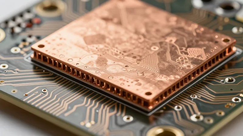
Strategic Selection of Microvia Configurations
In high-speed automotive SoCs, the transition from legacy through-hole designs to Microvia-in-Pad (VIP) and laser-drilled structures is critical. Advanced infotainment units require strict control over impedance discontinuities caused by parasitic capacitance. The selection between stacked and staggered microvia configurations fundamentally alters the return path efficiency and high-frequency resonance profiles.
| Configuration | Signal Integrity Benefit | Manufacturing Complexity |
|---|---|---|
| Staggered Microvias | Superior structural integrity and lower stress concentration. | Low |
| Stacked Microvias | Reduced trace routing length; minimizes signal reflection/capacitance. | High |
| Staggered on Ground Plane | Better power distribution path; lower loop inductance. | Medium |
Minimizing Parasitics in High-Speed Links
Stacked microvias are increasingly preferred for high-speed differential pairs (e.g., LPDDR5 or PCIe Gen4/5 lanes) because they enable a direct vertical path between layers, significantly reducing the parasitic stub length. However, achieving successful plating within stacked configurations requires precise control over aspect ratios to prevent voiding. Designers must ensure that the copper fill process complies with automotive reliability standards, particularly when exposed to harsh thermal cycling environments.
- Why is aspect ratio critical for laser microvias?
A high aspect ratio often leads to incomplete copper filling, creating reliability concerns in automotive applications and potential impedance mismatches due to air pockets or thinning. - How do stacked vias affect signal reflection?
By eliminating the horizontal trace segment between via transitions, stacked vias shorten the signal path and reduce localized capacitance, effectively pushing the parasitic resonance frequency outside the operational bandwidth. - Is there a DFM rule for via spacing?
Yes; maintain a minimum clearance of 3 mils between microvia pads to prevent plating overlap and ensure thermal expansion does not compromise dielectric isolation.
# Example constraint for high-speed signal routing
rule "Differential Pair Transition"
    layer_stack: "L1_L2_L3"
    via_config: "Stacked_Laser"
    max_stub_length: 0.15mm
    impedance_tolerance: +/- 5%
Optimizing Layer Stack-up for EMI and Signal Speed
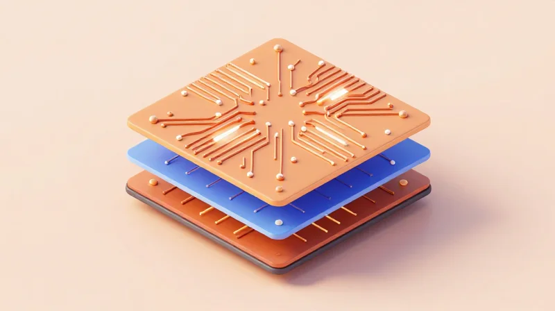
For HDI designs in automotive infotainment, the stack-up is the foundational element that determines the success of high-speed protocols like PCIe Gen 4/5 or automotive Ethernet. Achieving optimal EMI performance while maintaining signal speed requires a symmetric, ground-referenced structure that minimizes inductive loops and ensures return path continuity across transitions.
Strategic Ground Referencing and Return Path Management
In HDI layouts, high-speed signals must always reference a solid, contiguous ground plane. Interruptions in this reference, such as plane splits or excessive via anti-pads, create localized impedance discontinuities and increased electromagnetic radiation. Designers should prioritize a 'GND-Signal-GND' configuration where possible to contain fields and minimize crosstalk.
| Stack-up Strategy | EMI Mitigation | Signal Speed Benefit |
|---|---|---|
| Symmetric Layering | High (warpage reduction) | Medium (skew control) |
| Tight Coupling | Maximum (field containment) | High (impedance stability) |
| Embedded Capacitance | Excellent (high-freq noise) | High (PDN stability) |
Key Design Considerations for Impedance and Crosstalk
- How does trace spacing affect crosstalk in dense HDI?
As routing density increases, the '3W rule' is often insufficient. Utilize differential pair shielding and ensure the distance to the nearest reference plane is significantly smaller than the distance between adjacent signal traces. - What is the impact of dielectric material selection on signal speed?
Lower Df (dissipation factor) and Dk (dielectric constant) materials are mandatory for automotive infotainment to reduce signal attenuation and phase velocity variations across the board. - Why is symmetric stacking critical for automotive reliability?
Symmetric stack-ups balance internal stresses, preventing mechanical warpage during thermal cycling, which is essential to avoid microvia cracking in automotive-grade PCBs.
Precision Drill-to-Copper Clearances
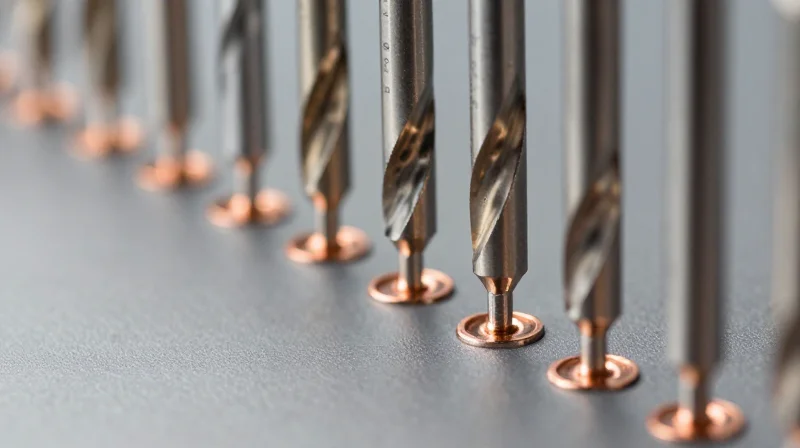
Optimizing Drill-to-Copper Clearance Margins
In automotive-grade HDI designs, the drill-to-copper clearance is the fundamental defense against short-circuits caused by drill wander and registration tolerances. As we shrink geometries to accommodate dense processing units, maintaining a robust gap between the mechanical drill bit or laser path and adjacent copper features becomes challenging. Designers must balance the desire for high-density routing with the reality of mechanical alignment tolerances, typically requiring a minimum clearance of 5-8 mils depending on the aspect ratio and board thickness.
Clearance and Reliability Comparison
| Feature | Standard HDI | Advanced Automotive |
|---|---|---|
| Drill-to-Copper (Min) | 6 mils | 8 mils+ |
| Registration Tolerance | +/- 3 mils | +/- 1.5 mils |
| Aspect Ratio | 1:1 | 1:0.5 |
Frequently Asked Questions
- Why is automotive clearance stricter than consumer electronics?
Automotive environments involve extreme thermal cycling and vibration. Larger clearances prevent potential dendritic growth and fatigue-induced shorts over the vehicle's 10-15 year lifespan. - How does drill wander impact my design rules?
Mechanical drills have a natural deviation factor. If your clearance is set too tight, the drill may clip an adjacent signal plane, leading to intermittent failures or complete board scrap. - Can laser-drilled microvias use smaller clearances?
Yes, laser processes offer higher precision than mechanical drilling, allowing for reduced clearance. However, copper-filled microvias often require specific annular ring targets to ensure plating integrity during subsequent processing.
Thermal Dissipation Strategies in Dense Layouts
Managing Heat Flux in High-Density Automotive SoCs
High-performance SoCs in automotive environments demand robust thermal dissipation because localized hotspots can degrade signal integrity and compromise long-term component reliability. Designers must balance high-density interconnect routing with low-thermal-resistance paths, ensuring heat is efficiently wicked away from the junction toward internal ground planes or external heatsinks without disrupting sensitive high-speed signal paths.
Thermal Via Strategy and Routing Conflicts
The implementation of thermal via arrays is critical for moving heat from the SoC thermal pad into the inner ground layers. In HDI designs, these vias must be carefully placed to minimize interference with high-speed differential pairs. To maintain board integrity, use non-conductive via filling (IPC-4761 Type VII) to allow for pad-in-via implementation, which optimizes thermal transfer while maintaining flat surfaces for component soldering.
| Strategy | Thermal Impact | DFM Consideration |
|---|---|---|
| Copper Pours | Distributes heat laterally | Balance with signal return paths |
| Thermal Vias | Conducts heat to inner planes | Watch for via-in-pad solder wicking |
| Embedded Heatsinks | Primary cooling interface | Ensure planar uniformity during lamination |
Frequently Asked Questions on HDI Thermal Management
- How do I prevent signal crosstalk when routing near thermal via arrays?
Increase clearance between high-speed traces and thermal via clusters. Utilize dedicated ground shielding or internal reference layers to isolate sensitive signals from the thermal current paths. - Should I use filled or capped vias under the SoC?
For HDI automotive boards, always use IPC-4761 Type VII (filled and capped) vias. This prevents solder wicking during assembly and provides a planar surface for the SoC thermal pad, reducing thermal interface material (TIM) voids. - Does copper thickness affect thermal dissipation in HDI?
Yes, but increasing copper thickness also increases etch requirements for fine-pitch HDI structures. Aim for 0.5 oz or 1 oz copper with high-thermal-conductivity base materials to balance heat management with routing precision.
Selecting Materials for Automotive Reliability
The Imperative of CTE Matching and Signal Stability
Automotive infotainment systems operate in harsh environments where temperature fluctuations can compromise interconnect reliability. The primary failure mode in HDI PCBs is via barrel cracking caused by mismatching Coefficients of Thermal Expansion (CTE). Engineers must select substrate materials that minimize the Z-axis CTE expansion to prevent strain on thin-wall microvias. Furthermore, maintaining stable Dielectric Constant (Dk) and Dissipation Factor (Df) across a wide frequency range is essential to preserve the integrity of high-speed signals generated by modern SoCs.
| Material Property | Automotive Requirement | Impact on Reliability |
|---|---|---|
| Z-Axis CTE | Low (<3.0% below Tg) | Reduces via barrel stress during thermal cycles |
| Glass Transition (Tg) | >170°C | Ensures structural integrity under high-heat operation |
| Dk/Df Stability | Consistent/Low | Prevents signal loss and impedance deviations |
Material Selection Criteria for High-Density Interconnects
- How does Dk stability affect automotive infotainment performance?
Stable Dk prevents impedance variations as environmental temperatures shift, which is vital for high-speed differential pairs routing from processors to displays. - Why is CTE matching crucial for HDI microvias?
HDI microvias are prone to fatigue. Matching the CTE of the dielectric to the copper plating minimizes mechanical stress on the via walls, preventing catastrophic open-circuit failures. - What role does the Df play in board selection?
A low Df reduces energy loss as heat within the dielectric, which is essential for managing the thermal envelope of tightly packed, high-performance processing modules.
By prioritizing materials with high Glass Transition (Tg) temperatures and ultra-low CTE, designers can significantly extend the Mean Time Between Failures (MTBF) for infotainment units. Standard FR-4 is generally insufficient; instead, high-reliability polyimide or advanced halogen-free ceramic-filled resins are recommended to ensure longevity in the automotive lifecycle.
DFM Verification Protocols

Automated DRC and Simulation Workflows
Modern automotive infotainment units require complex HDI architectures that exceed the capability of manual visual inspection. Automated Design Rule Checks (DRC) must be integrated into the ECAD environment to enforce stack-up specific constraints, including laser via aspect ratios, capture pad integrity, and inter-layer registration tolerances. Beyond static rules, manufacturing simulation tools—such as those analyzing solder paste deposition and plating distribution—are essential to forecast potential field failures in high-thermal-stress environments.
Critical DFM Verification Matrix
| Verification Category | Primary Metric | Automotive Risk |
|---|---|---|
| Via-in-Pad Plating | Void Percentage | Intermittent signal or thermal path failure |
| Annular Ring | Registration Offset | Drill breakout leading to layer shorting |
| Laser Drill | Aspect Ratio | Incomplete plating in microvias |
Common DFM Verification Questions
- How early should simulation start?
Simulation should commence at the floorplanning stage; late-stage verification often reveals fatal flaws that require complete design rework. - Are standard DRC scripts sufficient for HDI?
No. HDI designs demand specialized, multi-depth drill analysis scripts that account for the non-linear expansion of high-speed substrates under automotive temperature cycles. - How do I mitigate via-to-trace clearance violations?
Prioritize automated net-list driven spacing checks that dynamically adjust as you route dense BGA fan-outs, rather than relying on global constraint sets.
Bridging the Gap: Collaboration with Fabrication Partners
The Imperative of Early Engagement
For advanced automotive infotainment processing units, the complexity of HDI (High-Density Interconnect) routing, laser-drilled microvias, and precise impedance control often exceeds standard manufacturing specifications. Engaging your PCB fabricator at the conceptual design phase allows for a 'Design for Manufacturing' (DFM) alignment that reconciles high-speed performance requirements with the physical constraints of the fab line, preventing the 'over-specification' that leads to lower yields and increased costs.
Collaborative Design Verification
Formalizing the feedback loop between design engineers and fabrication engineers involves more than just sending Gerber files. It requires sharing stackup proposals, material specifications, and thermal management strategies well before the final tape-out. This proactive transparency allows fabricators to suggest adjustments to pad geometry, trace spacing, or build-up sequence, ensuring that the HDI features remain robust across the entire automotive production lifecycle.
| Collaboration Stage | Key Focus Area | Benefit of Early Input |
|---|---|---|
| Conceptual | Stackup Selection | Ensures CTE matching and thermal stability |
| Routing | Via-in-pad/Microvias | Optimizes plating quality and prevents voids |
| Pre-Production | Panelization | Maximizes material utilization and reduces unit cost |
Frequently Asked Questions on Fabricator Partnerships
- How often should we review design constraints with the fabricator?
Ideally, review at least three times: during the stackup proposal, midway through the layout phase for critical high-speed signals, and during final DRC sign-off. - What specific technical data should be shared early?
Always provide the stackup impedance target values, preferred material manufacturers for Dk/Df stability, and the expected current loads for power planes to ensure proper copper thickness management. - Does early collaboration guarantee defect-free prototypes?
While it does not guarantee perfection, it identifies latent manufacturing conflicts—such as potential drill aspect ratio violations—that would otherwise lead to failure during the prototyping stage.
By adhering to these rigorous DFM standards, automotive engineers can successfully balance high-speed performance with extreme reliability. Ready to optimize your next infotainment board design? Contact our engineering team today for a comprehensive design review or consultation on your next high-reliability project.
