
The modern vehicle cabin is evolving from a transport machine into a sophisticated mobile digital hub. As consumer demand for autonomous features and seamless connectivity grows, automotive engineers face a critical bottleneck: space. Discover why transitioning to HDI PCB technology is no longer optional, but essential for the future of in-vehicle infotainment.
The Shifting Paradigm of Automotive Cockpit Design
From Mechanical Dials to Digital Cockpits
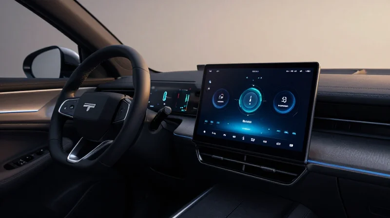
The modern automotive cockpit has undergone a profound metamorphosis, shifting from simple, isolated mechanical instruments to complex, interconnected digital ecosystems. Where once a driver relied on static analog needles and physical switches, today's driving experience is defined by high-resolution digital clusters, immersive heads-up displays, and expansive, touch-sensitive infotainment interfaces. This evolution is driven by the demand for seamless connectivity, advanced driver-assistance systems (ADAS), and a consumer desire for a 'smartphone-like' user experience within the vehicle.
Hardware Implications of the Digital Shift
The shift toward software-defined vehicles demands significantly higher computational power and data processing capabilities. Traditional cockpit architectures, reliant on discrete, bulky components, can no longer keep pace with these requirements. As functionality becomes more concentrated into smaller, high-performance computing units, the physical constraints on circuit boards become critical. Designers must now prioritize signal integrity, high-speed data transmission, and extreme spatial efficiency, leading to a critical divergence between traditional multilayer boards and advanced High-Density Interconnect (HDI) technologies.
| Feature | Traditional Multilayer Boards | HDI PCBs |
|---|---|---|
| Integration Density | Low to Moderate | High |
| Space Efficiency | Bulkier, requires more layers | Compact, thin, light |
| Signal Integrity | Limited at high frequencies | Superior for high-speed data |
| Primary Application | Basic control modules | Advanced infotainment & ADAS |
- Why is miniaturization necessary for modern cockpits?
Modern infotainment systems require complex processors and high-speed memory in tight, ergonomically constrained spaces, necessitating high-density hardware. - What role do HDI PCBs play in the user experience?
HDI PCBs allow for the high-speed data routing required to support lag-free, high-resolution touch displays and seamless connectivity, which directly enhances the perceived user experience. - Is the shift to HDI permanent?
Yes, as vehicles integrate more AI, deep learning, and advanced sensor fusion, the reliance on advanced, high-density manufacturing processes will only increase.
Anatomy of the Challenge: Why Traditional Multilayer Boards Fall Short
Physical and Performance Bottlenecks
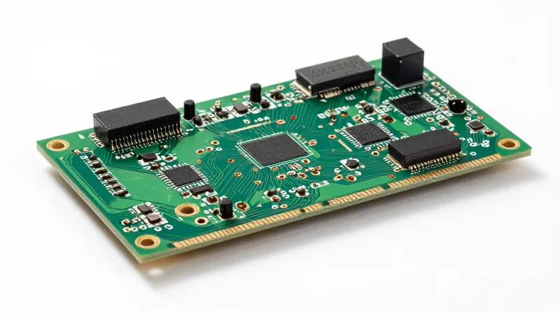
Traditional multilayer printed circuit boards (PCBs) were designed for an era of simpler automotive electronics. As infotainment systems move toward 4K displays, multi-camera ADAS feeds, and complex V2X communication, the inherent physical architecture of standard multilayer boards becomes a significant liability. These boards rely on through-hole technology and standard vias, which create large parasitic capacitances and inductances that degrade high-frequency signals.
| Feature | Traditional Multilayer | Performance Impact |
|---|---|---|
| Via Technology | Through-hole | Signal distortion at high frequencies |
| Component Density | Low/Moderate | Larger physical footprint |
| Trace Routing | Standard/Orthogonal | Increased electromagnetic interference |
| Layer Count | High required for complexity | Thermal dissipation challenges |
Why Traditional Designs Struggle
- Signal Integrity Limitations
Long through-hole vias act as antennas, causing impedance discontinuities that jeopardize high-speed data transmission required for modern infotainment processors. - Space and Weight Constraints
Modern cockpits demand smaller form factors. Standard boards require more layers and larger surface areas to accommodate the same number of I/Os that HDI can fit in a fraction of the space. - Thermal Management
As power densities rise, the thick stack-ups of traditional boards hinder effective heat dissipation, leading to localized hotspots and potential long-term component failure.
In the context of the modern infotainment stack, the limitation is not just about raw connectivity, but the ability to maintain clean data paths under thermal stress. The rigidity of traditional manufacturing processes—such as drill-to-copper clearances—prevents engineers from optimizing trace lengths, directly impacting the latency and reliability of the user interface.
Understanding HDI PCB Technology
Architectural Superiority of HDI Design
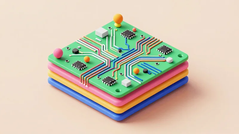
At its core, HDI technology differentiates itself from traditional multilayer boards through an architecture optimized for extreme component density. Unlike standard boards that rely on heavy through-hole vias, HDI boards utilize laser-drilled microvias, sequential build-up (SBU) processes, and significantly finer line widths. This configuration allows for shorter signal paths, reduced electromagnetic interference, and a much smaller footprint, which is critical for housing complex SoCs (System-on-Chips) and high-speed memory modules in compact automotive dashboards.
Key HDI Technical Advantages
| Feature | Traditional Multilayer | HDI PCB Technology |
|---|---|---|
| Via Structure | Mechanical Through-Hole | Laser-drilled Microvias (Blind/Buried) |
| Line Width/Spacing | Larger (>100um) | Ultra-fine (<50um) |
| Routing Density | Low to Medium | High Density |
| Component Pitch | Coarse | Fine-pitch BGA |
Understanding Microvias and Signal Integrity
The implementation of microvias is the most transformative element of HDI design. By eliminating the 'stub' effect common in through-hole vias—where excess copper barrel length acts as an unintended antenna—HDI boards significantly improve signal integrity at the high frequencies required by modern 4K displays and autonomous drive-assisted processing. This design shift ensures that high-speed data packets move with minimal degradation, a prerequisite for stable, high-bandwidth infotainment performance.
Frequently Asked Questions
- How does sequential build-up (SBU) improve reliability?
SBU allows for the construction of layers in stages, enabling the creation of intricate via structures that would be physically impossible in traditional boards, resulting in a more robust and compact layered architecture. - Why are finer line widths essential for modern cockpits?
Finer traces allow for more connections within a smaller surface area, enabling the use of high-pin-count processors and DDR memory while maintaining strict EMI control and thermal management standards. - Does HDI technology increase manufacturing complexity?
Yes, HDI requires advanced laser drilling, precise registration, and specialized imaging, which increases manufacturing precision but ultimately reduces total board size and allows for higher overall system integration.
Enhanced Signal Integrity for High-Speed Data

The Physics of Signal Integrity in Infotainment Systems
As automotive infotainment systems evolve to support high-definition video, multi-camera ADAS feeds, and real-time connectivity, the demand for high-speed signal integrity grows exponentially. HDI PCBs address these requirements by minimizing the physical distance signals must travel and reducing the reactive elements that impede high-frequency performance.
Mitigating Parasitic Capacitance and Inductance
In traditional multilayer boards, long signal traces and deep via barrels act as unintentional antennas and capacitors, causing signal reflection and EMI. HDI technology employs microvias, which significantly decrease the inductive loop area. By moving from through-hole vias to laser-drilled microvias, engineers can drastically lower parasitic capacitance, ensuring cleaner, high-speed data transmission without signal degradation.
| Feature | Traditional Multilayer | HDI Technology |
|---|---|---|
| Via Structure | Through-hole (Long) | Microvia (Short/Blind/Buried) |
| Parasitic Effects | High (significant reflection) | Low (minimal impedance mismatch) |
| Signal Path | Complex/Longer routing | Optimized/Shorter paths |
Key Considerations for High-Speed Design
- How do microvias improve impedance control?
Microvias offer a significantly reduced physical length compared to standard vias, which minimizes the discontinuity in transmission lines, allowing for more precise impedance matching at high frequencies. - Does HDI layout impact EMI radiation?
Yes, by enabling shorter signal paths and better ground plane integration, HDI boards reduce the inductive loop area, which directly correlates to lower electromagnetic interference in dense automotive environments. - Why is layer-to-layer registration accuracy critical?
In high-speed infotainment, trace impedance depends on consistent dielectric spacing; HDI manufacturing processes provide higher registration precision, preventing signal skew between differential pairs.
Supporting Autonomous Sensor Integration
Enabling Compact Sensor Fusion Architectures
The transition to autonomous features requires a massive increase in raw sensor data—from LiDAR to ultrasonic and high-resolution cameras. Traditional multilayer boards, limited by wider trace spacing and larger via structures, occupy too much physical space to accommodate the dense processing requirements of ADAS and infotainment modules. HDI technology shifts the paradigm by utilizing microvias and laser-drilled interconnects, allowing for significantly higher component density. This miniaturization is the catalyst for localized processing, where AI inference engines can sit closer to the sensor, reducing latency and overall system footprint.
Comparison of PCB Integration Capabilities
| Feature | Traditional Multilayer | HDI Technology |
|---|---|---|
| Via Diameter | Large (Mechanical) | Small (Laser Microvias) |
| Trace Density | Low | High |
| Component Pitch | Coarse | Fine (BGA/CSP) |
| Sensor Integration | Limited/Remote | High/Localized |
Key Considerations for Autonomous System Design
- How does HDI improve AI processing speed?
By allowing shorter signal paths and closer proximity between the sensor data input and the AI processing chip, HDI minimizes signal flight time and inductance, which is critical for real-time inference. - Does HDI support higher thermal management efficiency?
Yes, through the use of stacked microvias, heat can be more effectively transferred through internal layers to dedicated ground planes or heat sinks, preventing localized hotspots near critical AI processors. - Is HDI reliability suitable for automotive environments?
When manufactured to automotive-grade standards, HDI boards utilize advanced materials that offer superior mechanical robustness, vibration resistance, and thermal cycle durability compared to standard rigid boards.
Reliability and Thermal Management in Harsh Environments
Thermal Dynamics and Mechanical Durability
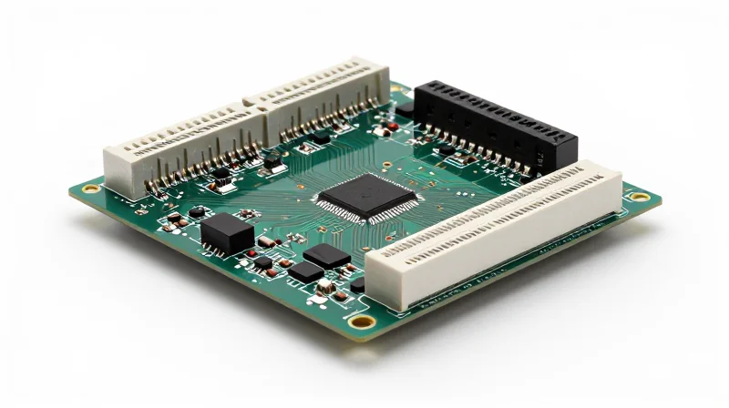
Modern automotive infotainment systems are subjected to extreme temperature cycles and persistent mechanical vibrations. HDI PCBs address these challenges through a lower profile and a reduced coefficient of thermal expansion (CTE) mismatch compared to bulky traditional boards. By utilizing laser-drilled microvias rather than mechanical through-holes, HDI boards minimize the risk of via-barrel cracking during rapid thermal cycling, a critical failure point in high-heat vehicle environments.
| Feature | Traditional Multilayer | HDI PCB |
|---|---|---|
| Thermal Stress Handling | Higher risk due to hole aspect ratio | Improved via-fill and structural integrity |
| Vibration Resistance | Prone to fatigue at solder joints | Lower mass allows better vibration tolerance |
| CTE Management | Higher board-level warping | Stable dielectric thickness and balanced copper |
Reliability Metrics in Harsh Conditions
- How do microvias handle thermal expansion?
Because microvias are small and shallow, they generate less stress on the surrounding dielectric material during thermal expansion, significantly extending the service life of the interconnect. - Does the smaller footprint improve vibration resistance?
Yes, reducing the physical board size decreases the mechanical lever arm effect, which lowers the amplitude of vibrations transferred to sensitive solder joints and BGA components. - What role does substrate material play in reliability?
HDI manufacturing utilizes high-Tg (glass transition temperature) materials that maintain rigid mechanical properties even when cabin temperatures exceed 125°C, ensuring consistent electrical paths.
Cost-Efficiency and Scalability in Manufacturing
Economic Dynamics of HDI Adoption
While traditional multilayer boards (MLBs) often carry lower unit costs in legacy systems, the transition to HDI technology offers significant cost-efficiency gains when factoring in system-level integration. By utilizing Micro-via technology and build-up processes, HDI boards reduce the total number of layers required, effectively shrinking the board footprint. This reduction in physical space lowers the bill of materials (BOM) cost for housing, cabling, and mechanical structural supports, proving that the premium on HDI fabrication is offset by the overall system downsizing.
| Metric | Traditional MLB | HDI Technology |
|---|---|---|
| Layer Count | High (12-20+) | Low (6-10) |
| Component Density | Standard | Ultra-High |
| System Footprint | Large | Compact |
| Integration Flexibility | Moderate | Advanced |
Scalability and Future-Proofing Infotainment Systems
Automotive OEMs must balance immediate production costs against the need for hardware that supports over-the-air (OTA) updates and evolving AI features. HDI PCBs facilitate this scalability by providing the necessary high-speed routing capabilities and signal integrity required by next-generation processors. As infotainment requirements shift from media consumption to complex sensor-fusion processing, the ability to upgrade processing power without re-designing the entire vehicle chassis architecture becomes a critical economic advantage.
Frequently Asked Questions
- Does HDI technology always result in higher production costs?
Not necessarily; while fabrication per board is more expensive, the total system-level cost is often lower due to reduced layer counts and smaller mechanical enclosure requirements. - How does HDI support long-term scalability?
HDI architectures allow for more efficient signal routing and power delivery, enabling OEMs to fit more powerful computing modules into the same footprint as the vehicle evolves. - Is the transition to HDI feasible for mid-range vehicle models?
Yes, as supply chain volume increases and manufacturing processes mature, the cost gap between HDI and standard MLBs is narrowing, making it increasingly viable for non-luxury segments.
Future-Proofing Your Electronic Assemblies
Strategic Adaptation for HDI Integration
Future-proofing electronic assemblies is no longer optional in the automotive sector; it is a prerequisite for sustaining competitive lifecycles. As infotainment systems evolve into central compute hubs, the reliance on traditional multilayer boards introduces bottlenecks in signal integrity and thermal density. Design engineers must transition toward High-Density Interconnect (HDI) structures that utilize micro-vias and finer line widths to enable sophisticated SoC (System on Chip) implementations.
| Design Factor | Traditional Multilayer | HDI Implementation |
|---|---|---|
| Component Density | Moderate (Limited by via pitch) | High (Supports ultra-fine pitch BGA) |
| Signal Integrity | Lower (Higher parasitic inductance) | Higher (Shorter routing paths) |
| Scalability | Rigid (Size constraints) | Dynamic (Modular HDI sub-layers) |
Key Considerations for Future-Ready Designs
- How does material selection impact long-term HDI reliability?
Utilizing low-loss, high-Tg (glass transition temperature) laminates is essential to combat thermal expansion stresses during high-speed data transmission. - Why is layer stack-up optimization critical for future upgrades?
A well-planned HDI stack-up allows for modular component placement, ensuring that core processing units can be upgraded in subsequent iterations without a full PCB redesign. - What role do micro-vias play in future-proofing?
Micro-vias significantly reduce the via-stub effect, providing the necessary signal cleanliness required for emerging high-bandwidth standards like PCIe Gen 5 and beyond.
To effectively future-proof, engineers should prioritize a 'design-for-manufacturing' (DFM) approach that accounts for the tighter tolerances of HDI while leveraging software-defined vehicle architectures. By reducing the reliance on oversized, legacy boards, manufacturers create the physical headroom necessary for future AI-driven feature integration and over-the-air updates.
As the automotive industry pushes the boundaries of cockpit digitalization, the superiority of HDI PCBs over traditional multilayer boards becomes undeniable. By prioritizing signal density and thermal stability, manufacturers can deliver a superior user experience while maintaining structural efficiency. Contact our engineering team today to learn how we can help integrate high-performance HDI solutions into your next-generation automotive designs.
