Electric Vehicle Charging Management System PCB Solution
2025.07.22
The global shift towards electric vehicles (EVs) is undeniable, paving the way for a sustainable future. At the heart of this revolution lies efficient and reliable charging infrastructure. But what ensures the seamless flow of power and intelligent management of battery health? It's the sophisticated electronics within, particularly the Printed Circuit Boards (PCBs) that serve as the backbone of every Electric Vehicle Charging Management System. At Zero One Solution Limited, we understand these critical demands. As a leading PCB solution provider specializing in rapid prototyping and comprehensive one-stop services from design to assembly, we are poised to empower your innovations in the EV charging space. This article delves into the intricate world of EV charging system PCBs and how our expertise provides the definitive solution.
The Electrifying Core: Understanding EV Charging Management Systems
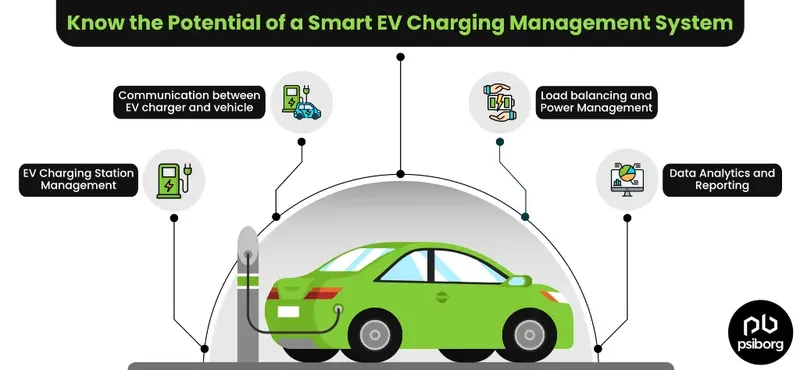
EV Charging Management System
At the heart of every electric vehicle (EV) charging experience lies the Charging Management System (CMS), a sophisticated network of electronic components orchestrating the seamless flow of power. These systems are not merely conduits of electricity; they are intelligent control centers that ensure safe, efficient, and reliable charging. The Printed Circuit Boards (PCBs) within these systems are the unsung heroes, providing the essential foundation upon which this advanced technology is built. They are the lifeblood of the system, integrating and connecting various components to enable the safe and efficient transfer of electrical energy from the power grid to the EV battery. Understanding the function of an EV Charging Management System (CMS) and its reliance on robust PCBs is essential for appreciating the complexity and ingenuity behind modern EV charging solutions.
The EV CMS comprises several critical components, each playing a vital role. The central processing unit (CPU) is the brain, making intelligent decisions based on sensor data and user input. Power conversion circuits, often utilizing high-power PCBs, transform AC power from the grid into DC power compatible with the EV's battery. Communication modules facilitate communication between the charger, the EV, and potentially the grid or other management systems. Safety circuits, including overcurrent protection and ground fault detection, prioritize the safety of both the user and the equipment. All these components are interconnected via a complex network of traces on the PCB, making the PCB the backbone of the system.
The PCBs in an EV charging system perform several crucial functions:
* **Power Distribution:** PCBs distribute high-voltage and high-current power efficiently and safely.
* **Signal Processing:** PCBs process signals from sensors, control circuits, and communication modules.
* **Control and Monitoring:** PCBs manage charging parameters, monitor system status, and control safety features.
* **Communication:** PCBs enable communication between the charger, the vehicle, and the charging network.
As the electric vehicle market continues to expand, so does the demand for advanced EV charging infrastructure. This in turn drives the need for sophisticated and reliable PCBs. From residential chargers to high-powered DC fast-charging stations, the design and manufacturing of these PCBs are critical to ensuring the performance, safety, and longevity of EV charging systems. At Zero One Solution Limited, we are committed to providing advanced PCB solutions for the EV charging market.
Navigating the PCB Challenges in Electric Vehicle Charging: Power Density, Thermal Management, and Reliability
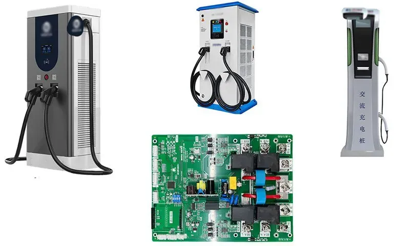
EV Charger PCB Board
The electric vehicle (EV) revolution places unprecedented demands on Printed Circuit Boards (PCBs) within charging infrastructure. Meeting these challenges is critical for ensuring the safety, efficiency, and longevity of EV chargers. This section delves into the primary hurdles encountered by PCBs in EV charging applications, including the need for high power density, effective thermal management, robust EMI/EMC compliance, signal integrity, and the capacity to endure harsh operating conditions. Successfully addressing these demands is essential for providing reliable and high-performance charging solutions.
EV chargers operate in demanding environments that necessitate specialized PCB design considerations. The major challenges include:
High Power Density EV chargers require PCBs that can handle significant power loads within compact spaces. This necessitates the use of advanced materials, such as thick copper PCBs, to efficiently distribute heat and minimize voltage drops. High power density also demands careful component placement and trace routing to prevent hotspots and ensure optimal performance.
Thermal Management Heat generation is a significant concern due to high currents. Effective thermal management solutions, including heat sinks, thermal vias, and advanced PCB materials (e.g., IMS), are crucial to dissipate heat and prevent component failure. Failure to manage heat can lead to reduced charger lifespan and potential safety hazards.
EMI/EMC Compliance EV chargers must comply with stringent electromagnetic interference (EMI) and electromagnetic compatibility (EMC) standards. PCB design plays a pivotal role in achieving compliance. This involves careful layout of traces, the use of shielding techniques, and the selection of components that minimize electromagnetic emissions and susceptibility. Failure to comply can lead to interference with other electronic devices and potential safety issues.
Signal Integrity The high-speed switching and complex control signals in EV chargers require careful consideration of signal integrity. This involves controlling impedance, minimizing signal reflections, and preventing signal degradation. Poor signal integrity can lead to communication errors and reduced charger efficiency.
Harsh Operating Environments EV charging stations often operate outdoors, exposing PCBs to extreme temperatures, humidity, and vibration. PCBs must be designed to withstand these harsh conditions. This includes the use of ruggedized components, conformal coatings for moisture protection, and robust mechanical designs to withstand vibration. These factors contribute to the overall reliability and longevity of the charging infrastructure.
Addressing these challenges requires a holistic approach to PCB design, manufacturing, and testing. Zero One Solution Limited specializes in providing tailored PCB solutions that meet the unique demands of EV charging applications. Our expertise ensures that your EV charging systems are not only efficient and reliable but also compliant with industry standards.
Zero One Solution: Your Partner in EV Charging Management PCB Solutions
PCB Design and Manufacturing
Zero One Solution Limited offers comprehensive PCB design, manufacturing, and assembly services tailored for the complex demands of Electric Vehicle (EV) Charging Management Systems. As a veteran in the Silicon Valley and with over a decade of experience in the PCB industry, we provide end-to-end solutions, ensuring your EV charging infrastructure benefits from cutting-edge technology and unparalleled reliability. Our expertise covers the entire product lifecycle, from initial design and prototyping to volume manufacturing, all optimized for the specific needs of the rapidly evolving EV market.
Our capabilities encompass the following key areas:
PCB Design and Layout We provide expert PCB design services, leveraging advanced CAD tools to optimize layouts for high-power, high-frequency applications. This includes meticulous consideration of signal integrity, power distribution, and thermal management to ensure peak performance and longevity of your EV charging systems. We adhere to industry best practices and standards to guarantee designs that meet or exceed regulatory requirements.
Rapid Prototyping We understand the importance of speed in the EV industry. Our rapid prototyping services enable you to quickly validate designs and accelerate time-to-market. With fast turnaround times, we help you test, iterate, and refine your designs efficiently, giving you a competitive edge in the market.
Manufacturing and Assembly Our state-of-the-art manufacturing facilities are equipped to handle complex PCB assemblies, including surface-mount technology (SMT) and through-hole components. We manage the entire manufacturing process, from component sourcing to final assembly, ensuring the highest quality and reliability of your EV charging PCBs. We also offer conformal coating and potting services to protect against harsh environmental conditions.
Testing and Quality Assurance We implement rigorous quality control processes, including Automated Optical Inspection (AOI), X-ray inspection, and functional testing, to ensure that every PCB meets the highest standards of quality and reliability. Our commitment to quality minimizes risks and maximizes the lifespan of your EV charging systems.
Supply Chain Management Leveraging our global network, we offer comprehensive supply chain management, ensuring access to a wide range of components and materials. This helps to mitigate supply chain disruptions and provides cost-effective solutions, enabling you to focus on innovation and product development.
With Zero One Solution Limited, you gain a partner dedicated to providing robust, reliable, and innovative PCB solutions for the EV charging sector. Our commitment to quality, combined with our expertise in design, manufacturing, and assembly, makes us the ideal choice for your Electric Vehicle Charging Management System PCB Solution needs.
High-Power and High-Frequency PCB Solutions for EV Chargers
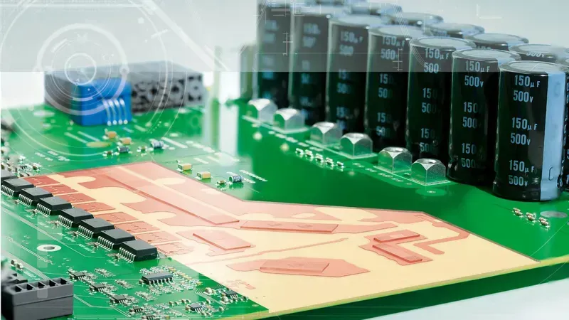
High-Power PCB
The evolution of Electric Vehicle (EV) charging infrastructure hinges on the development of robust, efficient, and reliable Printed Circuit Boards (PCBs). High-power and high-frequency applications demand specialized PCB technologies to manage significant current and voltage levels, ensuring operational safety and optimal performance. This section delves into the critical aspects of PCB design and manufacturing essential for modern EV chargers, focusing on Zero One Solution Limited's expertise in delivering cutting-edge solutions for this rapidly growing sector.
PCB Feature
Technical Specification
Zero One Solution's Expertise
Thick Copper PCBs
Copper thickness typically ranging from 2oz to 6oz or higher to handle high currents. Capable of carrying up to 100A or more.
Expertise in designing and manufacturing thick copper PCBs, ensuring optimal current carrying capacity and minimal thermal resistance. We use advanced etching techniques to maintain precise trace widths and spacing for high-current applications.
Impedance Control
Controlled impedance (e.g., 50 ohms or 75 ohms) to ensure signal integrity in high-frequency charging systems. Crucial for preventing signal reflections and ensuring data transmission.
Precision impedance control through careful selection of materials, stack-up design, and trace routing. We utilize advanced simulation tools to verify impedance characteristics, ensuring compliance with relevant standards.
Advanced Material Selection
Use of high-performance materials like FR4 or other specialized laminates with excellent thermal properties and high glass transition temperatures (Tg). These materials can handle high temperatures and ensure mechanical stability.
Strategic selection of PCB materials based on application requirements, including thermal conductivity, dielectric constant, and dissipation factor. We work with leading material suppliers to provide reliable and durable PCBs.
Thermal Management
Design features such as thermal vias, heat sinks, and copper pour planes to dissipate heat generated by power components. Effective thermal management is crucial for longevity and performance.
Implementation of advanced thermal management techniques, including designing thermal vias, incorporating heat sinks, and optimizing copper pour planes to manage heat effectively and prevent overheating.
Zero One Solution Limited leverages its extensive experience and state-of-the-art manufacturing capabilities to provide tailored solutions for high-power and high-frequency EV charger PCBs. Our commitment to quality, innovation, and customer satisfaction makes us a trusted partner for the EV industry.
Ensuring Safety and Reliability: Rigorous Testing and Quality Assurance for EV Charging PCBs
AOI Inspection
The safety and dependability of Electric Vehicle (EV) charging systems hinge on the uncompromising quality of their Printed Circuit Boards (PCBs). Zero One Solution Limited understands that the reliability of these critical components is non-negotiable, which is why we have established a comprehensive quality assurance program designed to exceed industry standards. Our commitment ensures that every PCB we manufacture for EV charging applications operates flawlessly, guaranteeing the longevity and safety of your charging infrastructure.
Our stringent quality control processes encompass several key stages:
Design for Manufacturability/Testability (DFM/DFT) Analysis: Before production begins, our engineers conduct thorough DFM/DFT analysis. This proactive approach identifies potential manufacturing issues and testability concerns early in the design phase, preventing costly rework and ensuring efficient production.
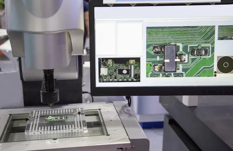
Automated Optical Inspection (AOI): AOI systems use high-resolution cameras to inspect PCBs for defects such as shorts, opens, and component placement errors. This automated process provides fast and accurate detection, ensuring that only high-quality boards proceed to the next stage.
X-ray Inspection: X-ray inspection is used for examining hidden solder joints and internal connections, particularly in densely populated PCBs. This technique allows us to verify the integrity of solder joints under components, crucial for high-power and high-frequency applications.
Functional Testing: We subject every PCB to rigorous functional testing. These tests simulate real-world operating conditions, verifying that the PCB performs as designed under various load and environmental conditions. This ensures that the charging system functions safely and efficiently.
Environmental Testing: EV charging systems are often exposed to harsh environments. Our PCBs undergo environmental testing, including thermal cycling, vibration testing, and humidity testing, to ensure they can withstand these conditions.
IPC Standards Compliance: Zero One Solution Limited adheres to the IPC (Association Connecting Electronics Industries) standards, ensuring that our manufacturing processes and quality control procedures meet the highest industry benchmarks.
By implementing these rigorous testing and quality assurance measures, Zero One Solution Limited provides EV charging PCB solutions that meet the highest standards of safety and reliability. Our commitment to quality ensures that your charging infrastructure operates flawlessly, supporting the growth of the EV market and contributing to a sustainable future.
Accelerating EV Charging Innovation with Rapid Prototyping
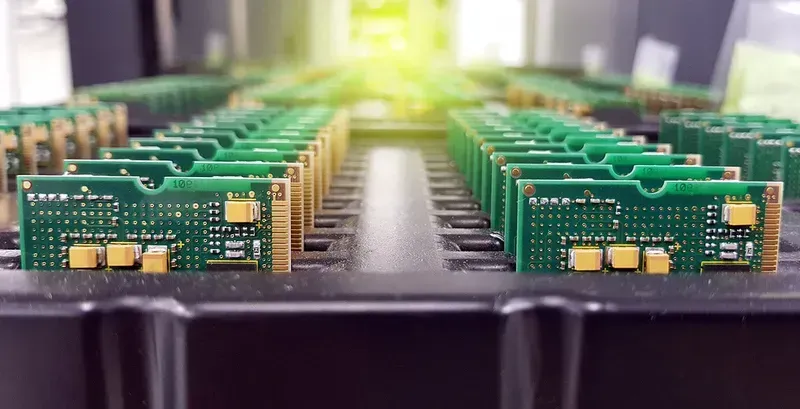
PCB Prototype
In the dynamic Electric Vehicle (EV) industry, speed is paramount. Rapid prototyping is not just an advantage; it's a necessity. It allows for quicker iterations, early identification of design flaws, and ultimately, faster time-to-market for innovative EV charging solutions. Zero One Solution Limited understands this critical need and offers rapid prototyping services specifically tailored for Electric Vehicle Charging Management System (EVMS) PCBs, enabling clients to stay ahead of the curve.
Rapid prototyping in the context of EV charging PCBs involves the swift creation and testing of initial PCB designs. This process encompasses several key steps:
Design and Layout Quickly translating the EV charging system's functional requirements into a PCB layout, considering high-power demands, signal integrity, and thermal management.
PCB Fabrication Manufacturing prototypes with accelerated turnaround times, often within days, using advanced manufacturing techniques and materials.
Assembly and Component Placement Efficiently assembling the PCB with necessary components, focusing on accurate placement and soldering.
Testing and Validation Rigorous testing of the prototype under simulated operating conditions to evaluate its performance, safety, and reliability.
Iteration and Optimization Implementing feedback from testing to refine the design, addressing any identified issues, and optimizing the PCB for peak performance.
Zero One Solution Limited's rapid prototyping capabilities provide significant benefits:
Reduced Time-to-Market Rapid prototyping drastically cuts down the product development cycle, enabling faster market entry and improved competitive advantage.
Early Problem Detection Prototyping allows for early identification of potential design flaws, which can be corrected before mass production, minimizing costly rework.
Enhanced Design Optimization Iterative prototyping enables engineers to refine PCB designs, leading to improved performance, efficiency, and reliability of the EV charging system.
Cost-Effectiveness While rapid prototyping may have higher upfront costs, the early detection and correction of issues reduce overall development expenses and the risk of costly errors in mass production.
By leveraging Zero One Solution Limited's rapid prototyping services, clients can confidently navigate the complexities of EV charging system development and bring cutting-edge solutions to market with speed and precision. This commitment to innovation and efficiency makes us a trusted partner for the future of electric mobility.
Custom PCB Solutions for Varied EV Charging Needs
Zero One Solution Limited understands that the Electric Vehicle (EV) charging landscape is not monolithic; it's a diverse ecosystem with varying power demands, form factors, and environmental considerations. Therefore, we specialize in providing custom PCB solutions designed to meet the unique challenges of each application, from compact residential chargers to robust public fast-charging stations and sophisticated Battery Management Systems (BMS).
Residential EV Chargers For home charging units, our PCBs are engineered for compactness, safety, and energy efficiency. We optimize designs for space-saving layouts and incorporate advanced features like surge protection and overcurrent protection, ensuring a safe and reliable charging experience for homeowners. We prioritize designs that meet all relevant safety standards and certifications, such as UL and CE.
Public Charging Stations Public charging stations demand high power handling capabilities and robust designs to withstand continuous use and environmental exposure. Our custom PCBs for these applications are built with high-quality materials, including thick copper layers for superior current carrying capacity, and are designed for efficient thermal management. We also provide solutions that enable seamless integration with payment systems, network connectivity, and user interfaces. We consider factors such as weather resistance and vandalism protection in our designs.
DC Fast Charging (DCFC) Stations DCFC stations require PCBs capable of handling extremely high voltages and currents. Zero One Solution Limited excels in providing specialized PCB solutions for these demanding applications. We utilize advanced materials like high-Tg (glass transition temperature) laminates to ensure thermal stability and reliability. Our designs incorporate impedance control, multilayer structures, and robust isolation techniques to meet stringent safety regulations and maximize charging speeds.
Battery Management Systems (BMS) The BMS is the brain of an EV's battery pack, requiring precise monitoring, control, and protection of the battery cells. Our custom PCBs for BMS applications are designed for high accuracy, low noise, and excellent reliability. We offer solutions for various BMS architectures, including centralized, distributed, and modular designs, catering to the diverse needs of EV manufacturers. Our BMS PCBs are engineered to meet stringent requirements for safety, efficiency, and longevity.
By offering tailored PCB solutions for these diverse applications, Zero One Solution Limited empowers clients to create innovative, reliable, and efficient EV charging systems that meet the specific demands of their target markets. Our commitment to customization ensures that your EV charging technology is optimized for performance, safety, and longevity, driving the future of electric mobility.
Partnering with Zero One Solution: Your Strategic Advantage in EV Charging PCBs
Choosing the right partner is paramount in the rapidly evolving Electric Vehicle (EV) landscape. Zero One Solution Limited offers more than just PCB manufacturing; we provide a strategic partnership designed to accelerate your success in the EV charging market. Our comprehensive capabilities, global reach, and unwavering commitment to quality make us the ideal choice for your EV Charging Management System PCB Solution needs.
Here's how partnering with Zero One Solution Limited benefits your EV charging projects:
Global Supply Chain Access Benefit from our strategically positioned global supply chain network. We ensure access to high-quality components and materials, mitigating supply chain disruptions and optimizing your project timelines.
Expert Engineering Support Our team of experienced engineers provides expert guidance from design to manufacturing. We offer DFM/DFA analysis to ensure manufacturability and optimize performance, reducing costs and accelerating time-to-market.
Commitment to Innovation We stay at the forefront of PCB technology, constantly adapting to the latest advancements in EV charging. Our commitment to R&D ensures that your projects benefit from cutting-edge solutions and the latest industry best practices.
Rapid Prototyping Capabilities Our rapid prototyping services enable quick iteration and validation of your designs. This fast turnaround allows you to swiftly respond to market demands and gain a competitive edge in the EV charging market.
Stringent Quality Control We adhere to rigorous quality control standards throughout the manufacturing process. Our comprehensive testing and inspection procedures guarantee the reliability and longevity of your EV charging PCBs.
Customized Solutions We offer tailored PCB solutions to meet your specific requirements, from residential chargers to public fast-charging stations. Our flexible approach ensures that we can accommodate your unique needs and project specifications.
Zero One Solution Limited is committed to your success in the dynamic EV charging market. Partner with us, and gain a trusted ally dedicated to delivering innovative, reliable, and high-performance PCB solutions. Contact us today to discuss your project requirements and discover how we can help you electrify the future.
Frequently Asked Questions (FAQs) about Electric Vehicle Charging System PCBs
Understanding the intricacies of Electric Vehicle Charging Management System (EVCMS) PCBs is crucial for ensuring the efficiency, safety, and reliability of EV charging infrastructure. This section addresses common questions to provide clarity on the critical aspects of these specialized PCBs.
What materials are typically used in EV charging system PCBs? EV charging system PCBs often utilize high-performance materials to withstand the demanding conditions of high-power applications. Common materials include FR-4, but for more advanced applications, materials like metal-core PCBs (MCPCBs) or those with high thermal conductivity may be employed to enhance heat dissipation. The choice depends on power levels, operating temperatures, and cost considerations.
What design considerations are most important for EV charging PCBs? Key design considerations encompass thermal management, high-voltage isolation, EMI/EMC shielding, and signal integrity. Proper layout techniques, such as wide traces for high currents, careful component placement to minimize thermal hotspots, and the use of ground planes for noise reduction, are essential. Additionally, selecting appropriate insulation materials and ensuring adequate creepage and clearance distances are critical for safety.
How is thermal management handled in EV charging PCBs? Thermal management is paramount due to the high power densities involved. Strategies include the use of MCPCBs with aluminum or copper cores for efficient heat transfer, strategically placed thermal vias to conduct heat away from sensitive components, and the incorporation of heat sinks or fans. Design software simulations are often used to optimize thermal performance.
What are the key aspects of EMI/EMC compliance for EV charging PCBs? To meet EMI/EMC compliance, designs must minimize electromagnetic interference. This involves using shielding techniques, such as enclosing the PCB in a metal enclosure, careful routing of high-frequency signals, and incorporating filtering components like ferrite beads and capacitors. Compliance with relevant standards (e.g., CISPR 11) is crucial to avoid interference with other electronic devices.
How is reliability ensured in EV charging system PCBs? Reliability is ensured through robust design practices, high-quality components, and rigorous testing. This includes Design for Manufacturability (DFM) and Design for Testing (DFT) analyses, Automated Optical Inspection (AOI), X-ray inspection, and functional testing under extreme conditions. Implementing these measures helps identify and address potential issues early in the manufacturing process, ensuring the longevity and safety of the PCBs.
How does Zero One Solution assist with the specific challenges of EV charging PCB design and manufacturing? Zero One Solution provides comprehensive support, including expert design assistance, material selection guidance, and advanced manufacturing capabilities. Our team helps clients navigate the complexities of EV charging PCB design, ensuring optimal performance, safety, and compliance. We specialize in rapid prototyping and offer customized solutions tailored to specific EV charging applications, supporting the rapid innovation needed in this fast-evolving industry.
In the rapidly evolving landscape of electric vehicles, the efficiency, safety, and reliability of charging infrastructure are paramount. As we've explored, the humble PCB stands as a monumental component within every EV Charging Management System, dictating its performance. Zero One Solution Limited is not just a PCB manufacturer; we are your strategic partner in accelerating innovation. With our veteran engineering expertise, rapid prototyping capabilities, and a commitment to unparalleled quality, we provide the robust, high-performance PCB solutions essential for the future of sustainable mobility. Don't let complex PCB challenges slow down your progress. Partner with Zero One Solution Limited to transform your EV charging concepts into market-ready realities. Contact us today to discuss your specific project requirements and leverage our decade of experience to power your success.