In an era increasingly powered by renewable energy and electric vehicles, the demand for reliable and efficient energy storage solutions has never been higher. At the heart of these sophisticated systems lies the Battery Management System (BMS), and its crucial component: the Printed Circuit Board (PCB). As a veteran engineer from Zero One Solution Limited, a leader in rapid prototyping and comprehensive PCB solutions since 2011, I've witnessed firsthand the transformative power of a well-designed BMS PCB. From ensuring optimal battery performance to safeguarding against critical failures, the quality of your BMS PCB is paramount. How can cutting-edge PCB solutions revolutionize your energy storage applications, and what makes Zero One Solution Limited your ideal partner in this journey?
The Crucial Role of PCBs in Battery Management Systems
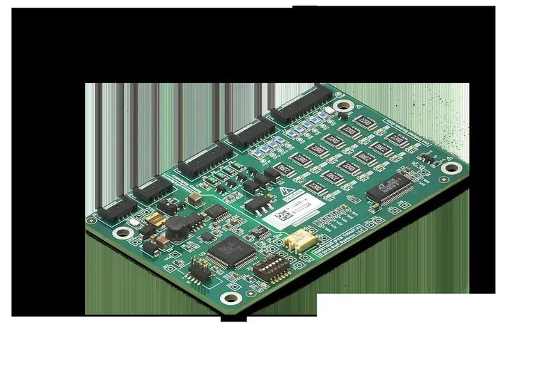
BMS Battery Management PCB Board
In the burgeoning landscape of energy storage, the Printed Circuit Board (PCB) serves as the indispensable backbone of any effective Battery Management System (BMS). Far more than just a circuit board, the PCB is the central nervous system that ensures the safety, longevity, and optimal performance of battery packs, whether in electric vehicles, grid-scale storage, or consumer electronics. Its design and manufacturing precision are paramount, directly influencing the BMS's ability to accurately monitor cell conditions, execute critical protection mechanisms, and facilitate robust communication within the energy storage ecosystem.
Precision Monitoring PCBs in BMS are engineered to precisely monitor individual cell voltages, temperatures, and current flow. This granular data is critical for identifying potential issues like overcharging, over-discharging, or thermal runaway before they escalate, safeguarding the battery pack and its environment. High-quality PCBs ensure the accuracy and reliability of these sensitive measurements, which are fundamental to effective battery management and overall system efficiency. According to a report by Grand View Research, the global battery management system market size was valued at USD 7.2 billion in 2022 and is expected to grow at a compound annual growth rate (CAGR) of 20.3% from 2023 to 2030, highlighting the increasing demand for robust BMS solutions built upon reliable PCBs.
Robust Protection Mechanisms The PCB integrates vital protection circuits that prevent damage to the battery and potential hazards. These include overcurrent protection, short-circuit protection, over-voltage, and under-voltage cut-offs. The layout and material selection of the PCB are crucial for handling high currents and dissipating heat efficiently, ensuring these protection mechanisms activate swiftly and reliably under extreme conditions. A poorly designed PCB can compromise these safeguards, leading to system failure or dangerous thermal events. Industry standards such as UL 1973 for stationary and motive batteries emphasize the importance of robust safety features, directly influenced by PCB design and manufacturing quality.
Seamless Communication A well-designed BMS PCB facilitates seamless communication between the battery pack and other system components, such as inverters, chargers, and central control units. It supports various communication protocols (e.g., CAN bus, SMBus) crucial for data exchange, system diagnostics, and firmware updates. Signal integrity on the PCB is critical to prevent data corruption and ensure reliable communication, which is essential for coordinated system operation and optimal energy utilization. Errors in communication, often due to poor PCB design, can lead to inefficiencies or even system shutdowns.
Data loss, system malfunctions, unreliable operation
Key Challenges in Energy Storage BMS PCB Design
Energy Storage PCB Thermal Management
Designing Printed Circuit Boards (PCBs) for Energy Storage Battery Management Systems (BMS) presents a unique set of engineering challenges that are critical to system performance, reliability, and safety. Unlike general-purpose PCBs, BMS boards operate in demanding environments, requiring meticulous consideration of high current pathways, effective thermal dissipation, robust signal integrity for precise data acquisition, and stringent electromagnetic compatibility (EMC) to prevent interference and ensure stable operation.
High Current Handling Energy storage systems involve significant power flow, necessitating PCB designs capable of safely and efficiently handling high currents. This requires wider copper traces, appropriate copper weight, and strategic component placement to minimize resistance and prevent excessive heat generation. Inadequate current handling can lead to trace burnout, reduced efficiency, and catastrophic system failure.
Thermal Management The operation of a BMS, particularly power components like FETs, generates heat. Effective thermal management is paramount to maintain optimal operating temperatures and ensure the longevity of components. This involves integrating thermal vias, strategically placing heat sinks, and optimizing PCB layout for efficient heat dissipation, often requiring multi-layer boards with dedicated thermal layers.
Signal Integrity Accurate voltage and current sensing, alongside reliable communication between various BMS components, depends on impeccable signal integrity. Noise, crosstalk, and impedance mismatches can corrupt critical data, leading to imprecise battery state estimations or erroneous protection actions. Careful routing, impedance control, and shielding are essential to preserve signal integrity in high-noise environments.
Electromagnetic Compatibility (EMC) BMS PCBs operate in an electrically noisy environment and must both avoid emitting harmful electromagnetic interference (EMI) and be immune to external EMI. This involves meticulous grounding schemes, proper filtering, careful component selection, and optimized layer stacking to ensure the system functions reliably without interfering with other electronic systems or being affected by external noise sources. Adherence to industry-specific EMC standards is crucial for market acceptance and regulatory compliance.
Zero One Solution's Expertise in BMS PCB Manufacturing
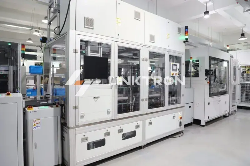
BMS PCB Manufacturing Line
Zero One Solution Limited stands at the forefront of Battery Management System (BMS) PCB manufacturing, leveraging over a decade of specialized experience to deliver high-quality, reliable solutions critical for advanced energy storage systems. Our unparalleled expertise in material selection, precise fabrication processes, and stringent quality control ensures that every BMS PCB we produce meets the demanding performance and safety requirements of modern energy storage applications. We understand that the integrity of the BMS PCB is paramount to the overall efficiency and longevity of battery systems, and our commitment to engineering excellence reflects this understanding.
Advanced Material Selection for Optimal Performance We meticulously select PCB base materials, such as high-Tg laminates and specialized copper foils, that can withstand the high temperatures, currents, and environmental stresses inherent in energy storage applications. This includes materials with superior dielectric properties for signal integrity and enhanced thermal conductivity for effective heat dissipation, crucial for preventing thermal runaway and extending battery life. Our material expertise ensures the foundational robustness of your BMS PCB solution, directly impacting its long-term reliability and safety.
Rapid Prototyping for Accelerated Energy Storage Innovation
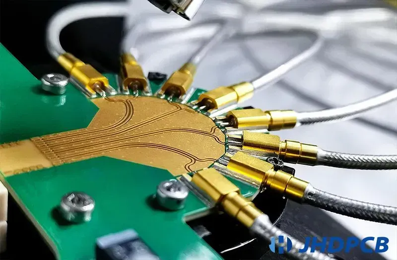
PCB Prototype Sample Testing
In the dynamic landscape of energy storage, accelerating the development cycle for Battery Management System (BMS) PCB solutions is paramount to gaining a competitive edge. Zero One Solution Limited's rapid-response R&D prototype manufacturing significantly streamlines this process, allowing innovators to iterate quickly, validate designs efficiently, and achieve faster time-to-market for their cutting-edge energy storage systems. This agility in prototyping is not merely a convenience but a strategic imperative, directly impacting the speed at which sustainable energy solutions can be deployed globally.
Reduced Development Cycles Our rapid prototyping capabilities compress the traditional PCB development timeline. By quickly moving from concept to physical prototype, design flaws are identified and rectified early, preventing costly delays in later stages of product development for energy storage BMS.
Enhanced Design Validation With rapid prototypes, engineers can conduct real-world testing and validation of their energy storage BMS designs. This iterative process allows for immediate feedback on performance, thermal characteristics, and signal integrity, ensuring optimal functionality before mass production.
Cost-Efficiency in R&D While often perceived as an added cost, rapid prototyping ultimately leads to significant cost savings. Early detection of design issues through quick iteration minimizes the need for expensive re-tooling or extensive modifications down the line, reducing overall R&D expenditure for energy storage PCB solutions.
Aspect
Traditional Prototyping
Zero One Rapid Prototyping
Turnaround Time
Weeks to Months
Days to Weeks
Iteration Speed
Slow, High Cost per Iteration
Fast, Lower Cost per Iteration
Risk of Rework
High
Low
Market Entry
Delayed
Accelerated
Design Flexibility
Limited once Production Starts
High Throughout R&D
By leveraging Zero One Solution Limited's rapid prototyping expertise, companies in the energy storage sector can transform their innovative ideas into market-ready products with unprecedented speed and efficiency, solidifying their position at the forefront of sustainable energy advancements.
Comprehensive Services: From Design to Assembly
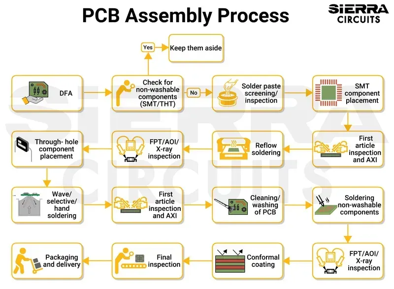
PCB Design to Assembly Process
At Zero One Solution Limited, we understand that bringing an energy storage battery management PCB solution to fruition requires more than just manufacturing expertise; it demands a seamless, end-to-end service that covers every phase of product development. Our integrated approach ensures that from the initial conceptualization of your energy storage PCB to its final assembly, you benefit from unparalleled efficiency, reduced lead times, and a single point of accountability, mitigating risks and accelerating your market entry.
Initial Design Consultation & Optimization We begin with a deep dive into your project requirements, offering expert design consultation for your energy storage PCBs. Our engineers collaborate with your team to optimize schematics, layouts, and component selection, ensuring the design meets performance, cost, and manufacturability targets from the outset. This early engagement is crucial for preventing costly revisions later in the development cycle.
Advanced PCB Manufacturing Leveraging state-of-the-art facilities in Shenzhen, we specialize in high-precision PCB manufacturing tailored for the stringent demands of energy storage BMS applications. This includes multi-layer PCBs, high-density interconnect (HDI) boards, and flexible PCBs, utilizing advanced materials that withstand high currents, dissipate heat effectively, and ensure signal integrity. Our processes adhere to IPC standards, guaranteeing superior quality and reliability.
Component Sourcing & Procurement Our extensive global supply chain network, reinforced by our Dubai branch, gives us a distinct advantage in sourcing high-quality, authentic components for your energy storage battery management PCB solutions. We manage the entire procurement process, from supplier qualification and negotiation to inventory management, ensuring timely availability of critical parts and protection against counterfeit components, all while optimizing costs.
Precise PCB Assembly (PCBA) Zero One Solution Limited provides comprehensive PCBA services, utilizing automated SMT and THT assembly lines to ensure precision and consistency. Our capabilities include fine-pitch component placement, BGA rework, and advanced soldering techniques. We employ rigorous quality control throughout the assembly process, including Automated Optical Inspection (AOI) and X-ray inspection, to ensure every assembly meets the highest standards of integrity and performance.
Rigorous Testing & Quality Assurance Before delivery, every energy storage battery management PCB undergoes a series of stringent tests, including in-circuit testing (ICT), functional testing (FCT), and environmental stress testing. This meticulous quality assurance process verifies the functionality, reliability, and safety of the assembled boards under various operating conditions, ensuring they are ready for immediate integration into your energy storage systems.
Ensuring Reliability and Safety in Energy Storage PCBs
PCB Quality Control Testing
In the demanding realm of energy storage, the reliability and safety of Battery Management System (BMS) PCBs are paramount. A single point of failure can lead to catastrophic consequences, from system downtime to thermal runaway. Zero One Solution Limited prioritizes stringent quality control, comprehensive testing protocols, and unwavering adherence to international industry standards to guarantee that our energy storage PCBs not only meet but exceed the most rigorous performance and safety benchmarks, ensuring the longevity and stable operation of your battery systems.
Rigorous Quality Control Measures Our commitment to reliability begins with a multi-stage quality control process. This includes meticulous incoming material inspection (IQC) to verify component integrity, in-process quality control (IPQC) at every manufacturing stage, and final quality assurance (FQA) before shipment. Automated Optical Inspection (AOI) and X-ray inspection are routinely employed to detect even the most minute defects, ensuring the highest level of build quality for energy storage BMS PCBs.
Comprehensive Testing Protocols for Performance and Safety Beyond visual inspections, we conduct extensive functional testing tailored to the specific demands of energy storage applications. This includes electrical tests like impedance control, continuity, and isolation testing to ensure signal integrity and power delivery. Thermal cycling and humidity testing simulate extreme operating conditions to verify long-term durability, while critical safety tests, such as short-circuit protection and overcharge/discharge protection, are rigorously validated to prevent potential hazards.
Adherence to Industry Standards and Certifications Zero One Solution Limited's manufacturing processes for energy storage PCBs strictly comply with global industry standards. We adhere to IPC (Association Connecting Electronics Industries) standards for PCB design, manufacturing, and assembly, ensuring consistent quality and performance. Our facilities are ISO 9001 certified, demonstrating our robust quality management system, and we ensure compliance with relevant environmental directives such as RoHS and REACH, underscoring our commitment to both product safety and environmental responsibility.
Global Reach and Supply Chain Advantage
Zero One Solution Limited's strategic global presence in Shenzhen, China, and Dubai, UAE, provides an unparalleled advantage in the energy storage battery management PCB solution landscape. This dual-location strategy ensures robust supply chain resilience, optimized logistics, and direct access to critical manufacturing ecosystems and emerging markets, enabling seamless resource acquisition and support for clients worldwide. By leveraging these hubs, we significantly reduce lead times and enhance responsiveness, a critical factor for the rapid development cycles inherent in energy storage innovations.
Location
Strategic Advantage
Impact on Energy Storage PCB Solutions
Shenzhen, China (Headquarters)
Global electronics manufacturing hub; access to advanced materials, fabrication technologies, and skilled labor; high-volume production capabilities.
Facilitates rapid prototyping and mass production of high-quality, cost-effective energy storage BMS PCBs; ensures access to cutting-edge PCB manufacturing processes and components.
Dubai, UAE (Branch Office)
Gateway to emerging markets in MENA and Africa; strong logistics infrastructure; economic diversification and innovation hub.
Enables efficient distribution and localized support for energy storage projects in rapidly expanding regional markets; enhances global supply chain diversification and risk mitigation.
Our integrated global supply chain management system further optimizes the procurement and delivery of energy storage battery management PCB solutions. This system meticulously coordinates raw material sourcing, component acquisition, manufacturing processes, and final product delivery across continents, ensuring efficiency and cost-effectiveness without compromising quality. This global network is crucial for navigating the complexities of international trade and supply chain dynamics, providing a competitive edge for our clients' energy storage projects.
How does Zero One Solution's global presence benefit lead times for energy storage BMS PCBs? Our strategic locations in Shenzhen, the heart of electronics manufacturing, and Dubai, a major logistics hub, significantly reduce lead times by ensuring immediate access to materials, advanced manufacturing capabilities, and streamlined global distribution channels. This dual-hub model minimizes transit times and customs complexities, accelerating project completion.
What specific supply chain advantages does Zero One Solution offer for energy storage PCB projects? We offer a resilient, diversified, and highly efficient global supply chain. This includes direct access to a vast network of vetted suppliers for specialized PCB materials and components, optimized logistics for global delivery, and regional support to navigate local market requirements and regulations. This comprehensive approach ensures supply stability and cost-effectiveness for energy storage PCB solutions.
Frequently Asked Questions about Energy Storage BMS PCBs
What are the primary considerations for designing a high-performance Energy Storage BMS PCB? Designing a high-performance Energy Storage BMS PCB necessitates a holistic approach, prioritizing robust current handling capabilities through optimized trace width and copper thickness, superior thermal management via strategic component placement and thermal vias, and exceptional signal integrity to ensure accurate data acquisition from battery cells. Additionally, designers must factor in electromagnetic compatibility (EMC) to prevent interference and select materials capable of withstanding harsh operating environments, such as high temperatures and humidity, to guarantee long-term reliability and safety. Compliance with industry standards like UL, CE, and IEC is also paramount from the outset to ensure certification readiness and market acceptance.
How does Zero One Solution Limited ensure the reliability and safety of Energy Storage BMS PCBs? Zero One Solution Limited prioritizes reliability and safety through a multi-faceted approach encompassing stringent material selection, advanced manufacturing processes, and comprehensive testing. We utilize high-Tg laminates and specialized copper foils for enhanced thermal performance and current capacity. Our fabrication processes adhere to IPC Class 2/3 standards, incorporating precise impedance control and advanced drilling techniques. Post-manufacturing, every BMS PCB undergoes rigorous testing, including Automated Optical Inspection (AOI), X-ray inspection for internal solder joints, In-Circuit Testing (ICT), and functional testing tailored to specific BMS requirements. This meticulous quality assurance protocol ensures compliance with critical safety standards and guarantees robust performance under demanding energy storage conditions.
What is the typical lead time for rapid prototyping of Energy Storage BMS PCBs with Zero One Solution Limited? Zero One Solution Limited is strategically positioned to offer industry-leading lead times for rapid prototyping of Energy Storage BMS PCBs. Leveraging our advanced manufacturing facilities in Shenzhen and optimized production workflows, we can typically deliver initial prototypes within 3-7 business days for standard designs, depending on complexity and material availability. This rapid turnaround is crucial for accelerating R&D cycles, enabling engineers to quickly validate designs, iterate, and bring their innovative energy storage solutions to market much faster, providing a significant competitive advantage.
Can Zero One Solution Limited assist with the design optimization of Energy Storage BMS PCBs? Yes, Zero One Solution Limited offers comprehensive support for design optimization of Energy Storage BMS PCBs as part of our one-stop service. Our experienced engineering team, with decades of expertise in PCB design and manufacturing, can provide valuable DFM (Design for Manufacturability) and DFA (Design for Assembly) feedback. This includes recommending optimal stack-ups, material choices, trace routing strategies for current handling and signal integrity, and component placement for thermal efficiency. By engaging early in the design phase, we help clients refine their BMS PCB designs to enhance performance, reduce costs, and improve manufacturability, ultimately ensuring a more robust and efficient final product.
What are the advantages of partnering with Zero One Solution Limited for Energy Storage BMS PCB solutions? Partnering with Zero One Solution Limited offers distinct advantages for Energy Storage BMS PCB solutions due to our specialized expertise, rapid prototyping capabilities, and global supply chain. Our deep understanding of BMS requirements ensures high-performance and reliable PCBs. Rapid prototyping accelerates time-to-market for innovative energy storage products. Furthermore, our strategic locations in Shenzhen and Dubai provide unparalleled access to a global supply chain, enabling competitive pricing, diverse material sourcing, and efficient logistics. This comprehensive approach, combined with our commitment to quality and customer service, positions us as an ideal partner for critical energy storage applications.
The future of energy storage hinges on robust, intelligent, and reliable Battery Management PCB solutions. Zero One Solution Limited, with our deep expertise, rapid prototyping capabilities, and global reach, is uniquely positioned to be your strategic partner in this evolution. We understand the intricate demands of energy storage systems and are committed to delivering PCBs that not only meet but exceed your performance and safety expectations. Partner with us to accelerate your product development, enhance the efficiency of your energy systems, and bring your innovative solutions to market faster. Contact Zero One Solution Limited today to discuss how our custom BMS PCB solutions can empower your next breakthrough.