As the world increasingly embraces renewable energy, photovoltaic (PV) systems are at the forefront of this green revolution. However, the efficient operation and longevity of these systems depend heavily on robust and reliable monitoring. At the core of every effective PV monitoring system lies a sophisticated Printed Circuit Board (PCB). Zero One Solution Limited, a leader in rapid prototyping and comprehensive PCB solutions, understands these critical demands. This article delves into how our specialized PCB solutions are empowering the next generation of photovoltaic monitoring systems, ensuring optimal performance and maximizing energy harvesting.
The Critical Role of PCBs in Photovoltaic Monitoring
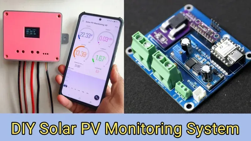
Photovoltaic Monitoring PCB
Printed Circuit Boards (PCBs) are the unseen backbone of photovoltaic (PV) monitoring systems, providing the foundational electronic platform essential for accurate data acquisition, seamless communication, and precise control within solar installations. Without high-performance, purpose-built PCBs, the sophisticated data capture, real-time analytics, and remote management capabilities crucial for optimizing solar energy production and ensuring system longevity would be impossible to achieve.
Data Acquisition Integrity PCBs facilitate the collection of critical data from various sensors, including voltage, current, temperature, and irradiance. Their design must ensure signal integrity, minimizing noise and interference to guarantee the accuracy of measurements, which directly impacts energy yield calculations and fault detection. According to a 2022 industry report, inaccurate data can lead to up to a 10% reduction in predicted solar farm efficiency over its lifespan due to delayed maintenance or suboptimal operation strategies.
Reliable Communication Pathways Modern PV monitoring systems rely on robust communication protocols (e.g., Modbus, Ethernet, Wi-Fi, LoRaWAN) to transmit data from inverters and sensors to central monitoring platforms. PCBs serve as the physical medium for these communication lines, requiring meticulous impedance matching and electromagnetic compatibility (EMC) design to ensure uninterrupted data flow and prevent signal loss or corruption, particularly across large-scale arrays and varying environmental conditions. A study by the Fraunhofer Institute for Solar Energy Systems indicated that communication failures, often linked to PCB issues, account for nearly 15% of system downtime in some PV installations.
Key Features of an Ideal Photovoltaic Monitoring PCB
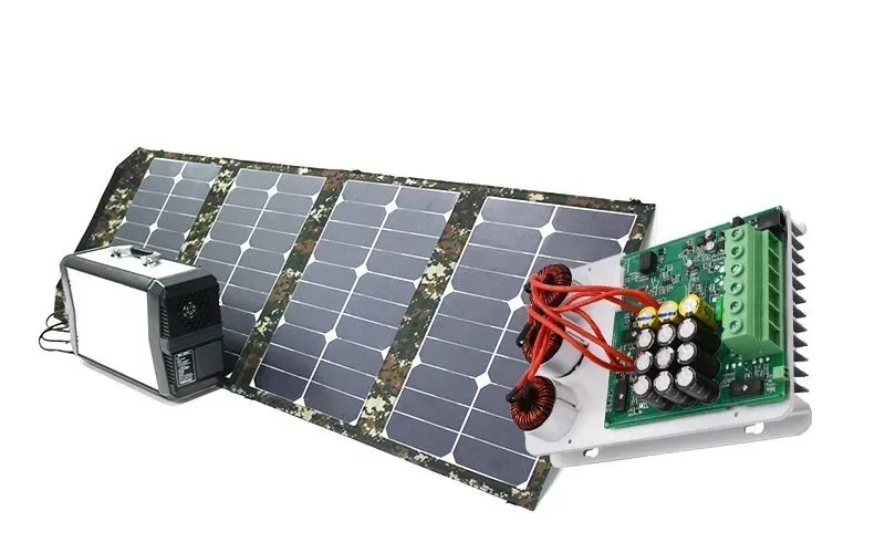
Solar Panel PCB Connection
An ideal Printed Circuit Board (PCB) for photovoltaic (PV) monitoring systems is engineered to ensure unwavering performance and data integrity in demanding outdoor environments. These PCBs are the backbone of reliable solar energy management, enabling precise data acquisition, efficient communication, and robust control. Key features revolve around ensuring durability, optimizing power consumption, maintaining signal integrity, and offering exceptional environmental resilience, which are paramount for the long-term operational success of any solar installation.
Feature
Description
Benefit for PV Monitoring Systems
Durability & Longevity
Robust design and material selection to withstand physical stress, vibration, and thermal cycling.
Ensures extended operational lifespan, reducing maintenance costs and system downtime in remote or harsh locations.
Low Power Consumption
Optimized circuit design and component selection to minimize power draw.
Maximizes system autonomy, especially in off-grid applications or where auxiliary power is limited, and reduces parasitic losses from the solar array.
High Signal Integrity
Careful layout, impedance matching, and shielding to prevent noise and interference.
Guarantees accurate data collection from sensors (voltage, current, temperature, irradiance), critical for performance analysis and fault detection.
Environmental Resilience
Selection of materials and conformal coatings resistant to extreme temperatures, humidity, UV radiation, and corrosive elements.
Maintains stable performance in diverse climates, from desert heat to freezing conditions, protecting sensitive electronics.
Ensures reliable data transmission to central monitoring stations, even in electrically noisy environments or during transient events.
Electromagnetic Compatibility (EMC)
Design adhering to strict EMC standards to minimize interference with other system components or external signals.
Prevents operational disruptions and ensures regulatory compliance, safeguarding data accuracy and system stability.
Scalability & Modularity
Design allowing for easy expansion and integration of additional sensors or functionalities.
Supports future system upgrades and adapts to evolving monitoring needs without requiring a complete system overhaul.
Cost-Effectiveness
Optimized manufacturing processes and material choices that balance performance with economic viability.
Provides a high-performance solution that is economically sustainable for large-scale deployments, maximizing ROI.
Zero One Solution Limited's Expertise in PV PCB Manufacturing
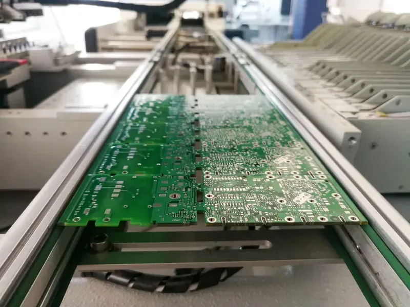
PCB Manufacturing Line
Zero One Solution Limited stands at the forefront of PCB manufacturing for photovoltaic monitoring systems, leveraging over a decade of specialized expertise to deliver high-performance, reliable solutions. Our unparalleled capability in rapid prototyping, advanced material selection, and precision manufacturing directly addresses the intricate demands of solar energy applications, ensuring optimal data acquisition and system longevity even in the most challenging environments.
Rapid Prototyping for Accelerated Development We understand the critical need for speed in product development. Our rapid prototyping service allows clients to swiftly iterate and validate their PCB designs for photovoltaic monitoring systems, significantly reducing time-to-market. This agile approach enables early detection of potential issues and facilitates quick design refinements, ensuring your solar innovations move from concept to reality with unmatched efficiency. Zero One Solution Limited's commitment to rapid response R&D prototype manufacturing means you can accelerate your product development cycles without compromising on quality or performance, a crucial advantage in the fast-paced renewable energy sector.
Advanced Material Selection for Durability and Performance The harsh environmental conditions faced by photovoltaic systems demand PCBs built with superior materials. Zero One Solution Limited specializes in selecting and utilizing advanced substrates and laminates that offer exceptional thermal management, UV resistance, and chemical stability. Our expertise extends to high-Tg materials for extreme temperatures, low-loss laminates for high-frequency data transmission, and specialized coatings for corrosion protection. This meticulous material selection process ensures that our PCBs for PV monitoring systems maintain their integrity and operational excellence over their extensive lifespan, providing a robust foundation for reliable solar energy management.
Capability
Benefit for PV Monitoring PCBs
Impact on System Performance
Rapid Prototyping
Accelerated design validation and iteration
Reduces time-to-market by up to 50%
Advanced Material Selection
Enhanced thermal management, UV resistance, and chemical stability
Ensures long-term reliability and operational excellence in harsh environments
Precision Manufacturing
Tight tolerances and consistent quality control
Minimizes signal interference and maximizes data accuracy
One-Stop Service
Streamlined design, manufacturing, and assembly
Reduces supply chain complexity and overall project costs
Custom PCB Design for Enhanced System Performance
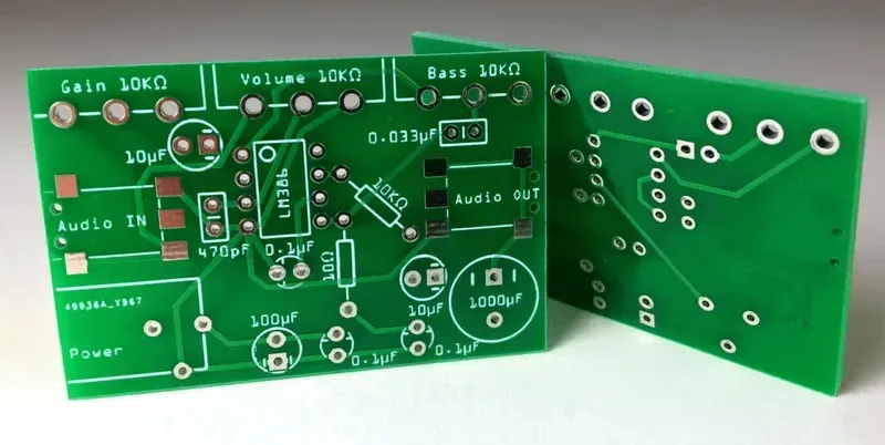
Custom PCB Design Engineer
Custom PCB design is paramount for optimizing photovoltaic (PV) monitoring systems, directly enhancing data accuracy, seamless system integration, and overall operational efficiency. While off-the-shelf solutions may offer initial cost savings, they often introduce performance compromises and integration challenges in the specialized and demanding environment of solar installations. A tailored PCB ensures that every component is optimally placed and interconnected, minimizing signal loss, reducing electromagnetic interference, and maximizing power efficiency—critical factors for precise data acquisition and reliable communication within a PV array.
Optimized Signal Integrity Custom designs meticulously manage trace lengths, impedance, and routing to prevent signal degradation, ensuring that sensor data (e.g., current, voltage, temperature, irradiance) is transmitted accurately to the monitoring unit. This precision is vital for effective system diagnostics and performance evaluation.
Enhanced Power Management Tailored PCBs can integrate sophisticated power management circuits designed for the specific power requirements and energy harvesting capabilities of PV systems. This leads to reduced power consumption, extended battery life for remote units, and improved overall system reliability.
Seamless Integration & Reduced Footprint A custom-designed PCB allows for precise form factor and connector placement, facilitating seamless integration with existing PV system components and enclosures. This reduces assembly time, minimizes the overall footprint, and often eliminates the need for costly adapters or custom cabling.
Environmental Resilience By selecting specific substrate materials and applying conformal coatings, custom PCBs can be engineered to withstand the harsh environmental conditions prevalent in solar installations, including extreme temperatures, humidity, UV exposure, and dust, ensuring long-term durability and performance.
Cost-Effectiveness in the Long Run While initial design costs may be higher, custom PCBs often lead to significant long-term savings. They reduce component count, simplify assembly, minimize failures, and optimize performance, leading to lower maintenance costs and a higher return on investment for the entire PV monitoring system.
Design Aspect
Off-the-Shelf PCB
Custom PCB for PV Monitoring
Signal Integrity
Compromised, potential for noise and data errors
Optimized for precise data acquisition and minimal interference
Power Efficiency
Generic, may lead to energy waste and shorter lifespan
Tailored for low power consumption and efficient energy harvesting
Integration
Often requires adapters, larger footprint, complex cabling
Seamless, compact, optimized for specific system architecture
Environmental Robustness
Limited protection, prone to environmental degradation
Engineered with specialized materials and coatings for harsh conditions
Long-term Cost
Lower initial, higher operational/maintenance due to sub-optimal performance
Higher initial, significant long-term savings through reliability and efficiency
Performance Reliability
Variable, dependent on environmental conditions and system load
Consistent, robust, designed for sustained peak performance
Quality Assurance and Reliability in Harsh Environments
PCB Environmental Testing
Ensuring the unwavering reliability of Printed Circuit Boards (PCBs) within photovoltaic (PV) monitoring systems, especially when deployed in demanding environmental conditions, is paramount. Zero One Solution Limited's commitment to rigorous quality assurance and exhaustive testing protocols is the bedrock of dependable performance, guaranteeing that our PCBs withstand the intense thermal fluctuations, high humidity levels, and significant electromagnetic interference inherent to solar installations. This meticulous approach minimizes downtime, maximizes data integrity, and extends the operational lifespan of critical monitoring infrastructure.
Environmental Challenge
Impact on PCB Performance
Zero One Solution's Mitigation Strategies
Extreme Temperatures
Component degradation, solder joint fatigue, material expansion/contraction leading to delamination.
Physical obstruction, reduced heat dissipation, potential short circuits.
Design for sealed enclosures, use of smooth surfaces, appropriate component spacing, and selective conformal coating application.
Why are quality assurance processes so crucial for PCBs in photovoltaic monitoring systems? Quality assurance processes are crucial because PV monitoring systems operate outdoors, exposed to extreme environmental conditions like fluctuating temperatures, high humidity, and UV radiation. Without stringent QA, PCBs can fail prematurely, leading to inaccurate data, system downtime, and significant financial losses. Robust QA ensures the longevity, reliability, and accuracy of the monitoring data, which is vital for optimizing solar farm performance and maintenance.
What specific tests does Zero One Solution Limited perform to ensure PCB reliability in harsh PV environments? Zero One Solution Limited employs a comprehensive suite of tests, including thermal cycling (e.g., -40°C to +85°C), humidity chamber testing, highly accelerated stress testing (HAST), vibration and shock testing, and extensive electromagnetic compatibility (EMC) and electromagnetic interference (EMI) testing. We also conduct visual inspections, automated optical inspection (AOI), X-ray inspection, and in-circuit testing (ICT) to verify manufacturing integrity and functionality.
How does Zero One Solution Limited address the challenge of electromagnetic interference (EMI) in PV monitoring PCBs? Addressing EMI involves a multi-faceted approach during design and manufacturing. We meticulously design PCBs with optimized ground planes, proper trace routing for signal integrity, and strategic component placement to minimize noise. We also implement shielding techniques, utilize differential signaling for sensitive lines, and ensure precise impedance control. Our final products undergo rigorous EMC/EMI testing to ensure compliance and stable operation in noisy electrical environments.
Are there specific material choices that contribute to the durability of your PCBs in outdoor solar applications? Absolutely. We select high-performance laminates with high glass transition temperatures (Tg) to withstand thermal stress. For moisture resistance, we may utilize specialized substrates and apply military-grade conformal coatings (e.g., acrylic, silicone, epoxy, or Parylene) that provide a protective barrier against humidity, chemicals, and contaminants. UV-resistant soldermasks are also employed to prevent degradation from prolonged sun exposure.
From Prototype to Production: Our One-Stop PCB Service
PCB Assembly Service
Navigating the journey from an innovative concept to a market-ready photovoltaic monitoring system demands a streamlined and efficient PCB development process. Zero One Solution Limited offers a comprehensive one-stop PCB service, meticulously designed to eliminate bottlenecks, reduce lead times, and ensure seamless transition from initial design and rapid prototyping through to mass manufacturing and final assembly. This integrated approach ensures consistency, quality, and accelerated market entry for your critical PV applications.
Conceptualization and Design Integration Our process begins with an in-depth understanding of your photovoltaic monitoring system's specific requirements. Our expert engineers collaborate closely with your team, translating conceptual designs into robust PCB layouts that prioritize signal integrity, power efficiency, and environmental resilience. We leverage advanced DFM (Design for Manufacturability) and DFA (Design for Assembly) principles from the outset to optimize designs for both performance and cost-effectiveness, reducing potential issues down the line.
Rapid Prototyping for Accelerated Validation Zero One Solution Limited specializes in rapid PCB prototyping, a cornerstone of agile product development. Utilizing cutting-edge fabrication techniques and high-precision equipment, we deliver functional prototypes swiftly. This allows for quick iteration, rigorous testing, and validation of design concepts, enabling engineers to identify and resolve potential issues early in the development cycle. Our rapid response capability significantly shortens the design-test-refine loop, crucial for time-to-market advantage in the competitive renewable energy sector.
Advanced Manufacturing and Assembly Once prototypes are validated, we transition seamlessly into scalable mass manufacturing. Our state-of-the-art facilities, equipped with automated SMT lines and advanced assembly technologies, ensure high-volume production with unwavering quality and precision. We adhere to stringent IPC standards and implement rigorous in-process quality control, including AOI, X-ray inspection, and functional testing, to guarantee every PCB meets the demanding specifications required for reliable operation in photovoltaic monitoring systems. Our global supply chain network ensures access to premium components, minimizing delays and optimizing costs.
Comprehensive Quality Assurance and Testing Quality is embedded at every stage. Before final delivery, all PCBs undergo a comprehensive suite of quality assurance tests, including electrical testing, burn-in tests, and environmental stress screening (ESS), to verify performance under various operating conditions. This exhaustive validation process guarantees the long-term reliability and durability of our PCBs, ensuring they withstand the harsh environments typical of PV installations, from extreme temperatures to high humidity and electromagnetic interference.
Logistics and Post-Production Support Beyond manufacturing, Zero One Solution Limited provides integrated logistics and post-production support. We manage global shipping and supply chain coordination to ensure timely delivery of your PCBs. Our commitment extends to ongoing technical support, addressing any post-delivery inquiries or operational challenges. This end-to-end service model ensures a hassle-free experience, allowing our clients to focus on their core innovation.
Future Trends and Innovations in Photovoltaic Monitoring PCBs
The evolution of photovoltaic monitoring systems is intrinsically linked to advancements in PCB technology. As the solar energy landscape shifts towards smarter, more interconnected, and highly efficient solutions, the PCBs at their core must evolve in tandem. Future trends in photovoltaic monitoring PCBs are centered on integrating cutting-edge technologies like the Internet of Things (IoT), artificial intelligence (AI)-driven analytics, and advanced sensor fusion, all designed to enhance data accuracy, predictive maintenance, and overall system autonomy. Zero One Solution Limited remains at the forefront, actively researching and adopting these innovations to provide future-proof PCB solutions that not only meet but anticipate the demands of next-generation solar energy infrastructure.
How is IoT integration transforming photovoltaic monitoring PCBs? IoT integration in PV monitoring PCBs enables seamless, real-time data exchange from individual solar panels and inverters to centralized cloud platforms. This allows for remote monitoring, predictive maintenance, and optimized energy output. PCBs are being designed with integrated Wi-Fi, LoRa, or cellular modules, requiring compact layouts, low power consumption, and robust signal integrity to support continuous, reliable connectivity across vast solar farms.
What role does AI play in the future of PV monitoring PCB design? AI will increasingly drive intelligent decision-making within PV monitoring systems. PCBs are evolving to incorporate more powerful, energy-efficient microcontrollers and dedicated AI accelerators capable of processing vast amounts of sensor data on-device (edge computing). This allows for real-time anomaly detection, performance optimization, and predictive fault identification, minimizing latency and reducing reliance on constant cloud connectivity.
How will advanced sensor fusion impact PCB design for solar applications? Advanced sensor fusion combines data from multiple sensors (e.g., temperature, irradiance, voltage, current, humidity, wind speed) to provide a more comprehensive and accurate understanding of system performance and environmental conditions. Future PV monitoring PCBs will need to accommodate a higher density of diverse sensor interfaces, ensuring excellent signal isolation, noise reduction, and efficient power distribution to support these integrated sensor arrays. This leads to more robust and accurate monitoring, enhancing system reliability and efficiency.
What are the challenges for PCBs in supporting these future PV technologies? Key challenges include managing increased data processing demands with lower power consumption, ensuring robust electromagnetic compatibility (EMC) in noisy solar environments, integrating diverse communication protocols, and maintaining miniaturization while enhancing functionality. PCBs must also be designed for extreme long-term reliability and thermal management to withstand harsh outdoor conditions over decades.
Frequently Asked Questions About Photovoltaic Monitoring System PCBs
Why are specialized PCBs critical for photovoltaic monitoring systems? Specialized PCBs are critical because photovoltaic monitoring systems operate in demanding outdoor environments, requiring boards that can withstand extreme temperatures, humidity, UV radiation, and electromagnetic interference. They must also ensure precise data acquisition from various sensors (voltage, current, temperature, irradiance), maintain signal integrity over long distances, and support robust communication protocols for reliable data transmission to central monitoring units. Standard PCBs often lack the necessary durability and performance characteristics for these specific challenges, leading to system inefficiencies or failures. For instance, high-temperature operation can degrade standard FR-4 laminates, while robust materials like polyimide or high-Tg epoxies are essential for longevity and stable electrical properties in PV applications. Additionally, efficient power management and low power consumption features are crucial for off-grid or battery-backed systems, directly influencing the choice of PCB components and design strategies.
What key design considerations are essential for Photovoltaic Monitoring System PCBs? Key design considerations for Photovoltaic Monitoring System PCBs include robust environmental sealing and conformal coating to protect against moisture and contaminants, selection of high-reliability components rated for industrial temperature ranges (-40°C to +85°C), and optimized layout for signal integrity to minimize noise and interference in analog and digital lines. Thermal management is also crucial, involving careful component placement and heat dissipation techniques to prevent overheating under direct sunlight. Furthermore, surge protection and EMI shielding are vital to safeguard sensitive electronics from lightning strikes and grid disturbances. Finally, power efficiency is a paramount consideration, necessitating designs that minimize quiescent current and optimize power conversion for extended operational life in remote or solar-powered installations.
How does Zero One Solution Limited ensure the reliability of PCBs in harsh PV environments? Zero One Solution Limited ensures reliability through a multi-faceted approach. We select high-performance base materials (e.g., high-Tg laminates, ceramic substrates) that maintain stable electrical and mechanical properties across wide temperature ranges. Our manufacturing processes include precise trace impedance control and robust solder joint integrity to withstand thermal cycling. We apply advanced conformal coatings and potting techniques for moisture, dust, and chemical resistance. Rigorous testing protocols, including thermal shock testing, humidity cycling, vibration testing, and accelerated life testing, simulate real-world harsh conditions. Additionally, our designs incorporate robust grounding schemes and shielding to mitigate EMI/EMC issues, crucial for accurate data transmission in electromagnetically noisy environments.
Can custom PCB designs improve the performance of a photovoltaic monitoring system? Absolutely. Custom PCB designs are instrumental in optimizing photovoltaic monitoring system performance by precisely tailoring the board to the unique sensor requirements, communication protocols, and power management needs of a specific application. This allows for superior signal integrity by minimizing trace lengths and optimizing routing for sensitive analog inputs, leading to more accurate data acquisition from PV panels and environmental sensors. Customization also enables efficient integration of specific microcontrollers, wireless modules (e.g., LoRa, cellular), and power conditioning circuits, optimizing power consumption and extending system battery life. Furthermore, a bespoke design can accommodate specialized form factors for easy installation and enhanced environmental protection, ultimately leading to a more reliable, efficient, and cost-effective monitoring solution adapted to its operational context.
What is the typical lead time for rapid prototyping of Photovoltaic Monitoring System PCBs? The typical lead time for rapid prototyping of Photovoltaic Monitoring System PCBs at Zero One Solution Limited varies based on design complexity, material availability, and layer count, but generally ranges from 3 to 7 business days for bare PCBs. For full assembly (PCBA), including component procurement and assembly, the lead time can extend to 7 to 15 business days. We leverage advanced manufacturing capabilities and a streamlined supply chain, especially from our Shenzhen hub, to significantly accelerate this process. Our emphasis on rapid prototyping allows clients to quickly test and iterate their designs, reducing time-to-market for innovative PV monitoring solutions. We also offer expedited services for urgent requirements, ensuring project timelines are met efficiently.
The transition to a sustainable energy future heavily relies on efficient and reliable photovoltaic systems, and robust monitoring is paramount to their success. Zero One Solution Limited is committed to being at the forefront of this evolution, providing the critical PCB solutions that power these vital monitoring systems. Our dedication to rapid prototyping, quality, and comprehensive service ensures that your PV projects benefit from the highest levels of performance and reliability. By choosing Zero One Solution Limited, you are partnering with a company that not only understands the intricacies of advanced PCB manufacturing but also shares your vision for a more sustainable world. Contact us today to discuss how our bespoke PCB solutions can elevate your photovoltaic monitoring capabilities and accelerate your journey towards energy independence and efficiency.