
In the fast-paced automotive sector, an inefficient seat heater controller isn't just a design flaw—it's a potential safety hazard and a costly manufacturing bottleneck. Designing for Manufacturability (DFM) is your primary defense against costly rework and field failures. This guide provides the technical roadmap to balancing thermal efficiency with mass-production reliability.
Understanding the Automotive Environment
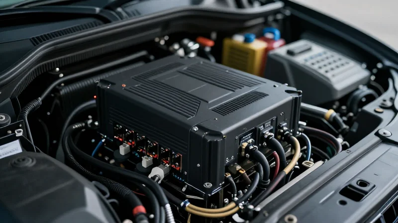
Navigating Automotive Environmental Rigors
The automotive seat heater control unit is located in a high-stress zone, directly underneath the occupant. Unlike cabin-grade electronics, these PCBs face extreme duty cycles, requiring Design for Manufacturing (DFM) strategies that prioritize robust physical construction and thermal management to prevent premature failure.
Key Environmental Stressors
| Environmental Factor | Primary Failure Mode | DFM Mitigation Strategy |
|---|---|---|
| Vibration | Solder joint fatigue | Underfill and secure component mounting |
| Temperature Cycling | CTE mismatch stress | CTE-matched substrates and thick copper |
| Chemical/Humidity | Corrosion/Dendritic growth | Conformal coating and sealed enclosures |
Addressing Design Uncertainties
- How does vibration affect controller longevity?
Constant micro-vibrations from the road transmit directly to the seat base, often causing fractures in large SMT solder joints. DFM guidelines dictate using corner staking or underfill for heavy components to distribute mechanical load. - Why is temperature cycling critical for seat heaters?
Rapid transitions between ambient cold starts and high-current heating phases create coefficient of thermal expansion (CTE) stresses, which can delaminate board layers. Using high-Tg FR-4 or metal-core PCBs helps stabilize the assembly. - What measures prevent chemical-induced shorts?
Fluids such as cleaning agents or spilled beverages can reach the controller. A stringent DFM approach requires specified keep-out zones for critical traces and the application of automotive-grade conformal coatings to prevent short-circuiting due to moisture.
Power Distribution Network Optimization
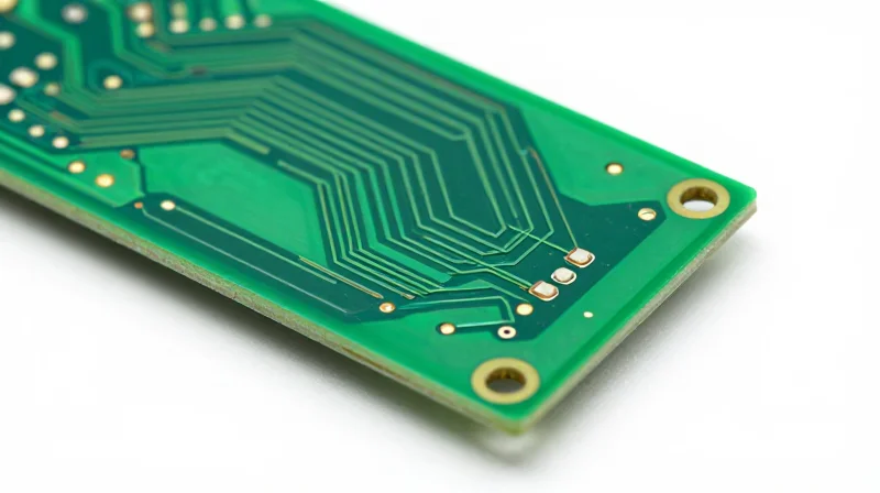
Trace Width and Current Carrying Capacity
For seat heater modules, trace design is dictated by high continuous current demands. Designers must utilize the IPC-2221 or IPC-2152 standards to calculate minimum trace widths, factoring in the maximum allowable temperature rise. To minimize board real estate while maintaining thermal integrity, prioritize inner layers for signals and reserve heavy copper outer layers (typically 2oz or higher) for the primary power path.
Minimizing Parasitic Resistance
Parasitic resistance in traces generates localized heat and causes voltage drops, which can lead to inefficient heating cycles and component stress. Implement these strategies to maintain signal integrity:
- Use Copper Pours
Replace narrow traces with broad copper planes to reduce impedance and improve heat dissipation into the substrate. - Strategic Via Stitching
Utilize arrays of thermal vias under power MOSFETs and along high-current paths to lower the total resistance between PCB layers. - Solder Mask Removal
Consider exposed copper areas or solder-wicking reinforcements on high-current rails to manually increase the thickness of the current-carrying path.
Comparison of Copper Weight for Power Rails
| Copper Weight | Current Capacity | Thermal Impact | Cost Implication |
|---|---|---|---|
| 1.0 oz | Low | Higher resistance, heat rise | Baseline |
| 2.0 oz | Moderate | Balanced performance | Moderate Increase |
| 3.0+ oz | High | Excellent heat sinking | Premium |
Managing PWM Switching Noise
High-frequency PWM switching introduces significant EMI risks. Decoupling capacitors must be placed as close as possible to the MOSFET driver pins. Furthermore, utilize a Kelvin connection for current sense resistors to ensure accurate feedback without the interference of high-current trace resistance.
Advanced Thermal Management Strategies
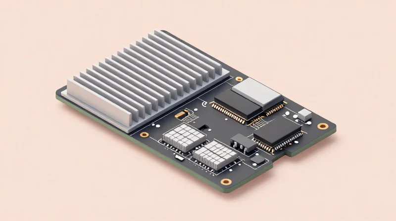
Advanced Thermal Management Strategies
For seat heater controllers operating in high-current PWM modes, thermal management is not merely an auxiliary feature but a critical reliability requirement. Effective dissipation relies on reducing junction-to-ambient thermal resistance through optimized PCB geometry, ensuring MOSFETs remain within safe operating areas despite continuous thermal cycling.
Copper Pour and Thermal Via Engineering
Maximizing the copper surface area connected to MOSFET thermal pads is essential. By utilizing multi-layer stack-ups, designers can tie the primary heat source to internal ground or power planes. Implementing a dense 'via farm' directly under the device footprint is the most effective way to transfer heat to bottom-side copper layers, significantly reducing the thermal path length.
| Strategy | Primary Benefit | DFM Consideration |
|---|---|---|
| Via-in-Pad | Lowest thermal resistance | Requires epoxy plugging to prevent solder wicking |
| Thick Copper (2oz+) | Higher current/heat capacity | Impacts etch time and fine-pitch resolution |
| Thermal Vias | Vertical heat transfer | Grid spacing must accommodate drill/plating tolerances |
Frequently Asked Questions on Thermal Reliability
- How do thermal vias impact DFM assembly?
While essential, improperly placed vias can cause solder wicking during reflow. Always specify via-plugging (capped or filled) for vias located within the MOSFET solder mask opening. - Is a standalone heat sink always necessary?
Not necessarily. If the PCB copper pours are correctly calculated for the thermal load and thermal resistance, the board itself can serve as a heat sink. However, for continuous high-load seat heating, aluminum-backed PCBs or clip-on heat sinks provide a better safety margin. - What is the role of thermal interface materials (TIM)?
TIMs bridge the gap between the component package and the heat sink or enclosure, minimizing interfacial air voids that otherwise trap heat and cause premature device degradation.
Stack-up Design for Signal Integrity
Strategic Layer Stack-up for Noise Mitigation
In seat heater control modules, the primary integrity challenge arises from the high-frequency PWM switching of MOSFETs coupled with sensitive low-voltage sensing circuitry. To prevent EMI coupling, a minimum of a four-layer stack-up is recommended. This approach separates high-current power stages from signal-level control loops using dedicated ground planes, effectively providing a low-impedance return path for high-speed switching transients.
Recommended Layer Assignments
| Layer | Function | Purpose |
|---|---|---|
| Top | Power & Components | High-current MOSFET paths and thermal pours |
| Inner 1 | Ground Plane | Continuous return path to minimize loop area |
| Inner 2 | Control/Signal | Isolated routing for logic and ADC feedback |
| Bottom | Power/Ground/Logic | Secondary thermal dissipation or auxiliary signals |
Key Design Considerations for Signal Integrity
- How do I minimize loop inductance in PWM circuits?
Always place a dedicated reference plane directly adjacent to the high-current switching traces. This forces return currents to flow directly beneath the signal, minimizing the physical loop area and significantly reducing magnetic field emissions. - Should I use split ground planes?
Avoid splitting ground planes whenever possible. Splits create high-impedance discontinuities that force currents to wrap around, potentially creating large antenna loops that radiate EMI. Use physical separation and spatial component placement instead. - What is the impact of via stitching on signal integrity?
Via stitching is essential when transitioning signals between layers. By placing ground stitching vias adjacent to signal vias, you maintain a consistent return path impedance, reducing signal reflections and crosstalk.
By maintaining these stack-up conventions, engineers can significantly reduce the risk of board-level interference. Adherence to these guidelines ensures that the control module remains compliant with automotive EMC standards such as CISPR 25 while simultaneously reducing the cost of iterative testing cycles.
Component Placement and Assembly Rules
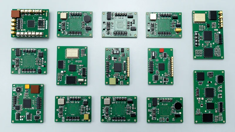
SMT Placement Strategy for High-Current Circuits
To ensure reliable high-current performance, prioritize the proximity of power components to the load while maintaining strict thermal separation from sensitive control logic. Consistent orientation of passive components, particularly current-sensing resistors and decoupling capacitors, is essential for repeatable SMT reflow performance and simplified AOI (Automated Optical Inspection) programming.
Preventing Common Assembly Defects
| Defect Type | Primary Root Cause | DFM Mitigation Strategy |
|---|---|---|
| Tombstoning | Uneven solder wetting/thermal profile | Ensure symmetric land patterns and thermal relief connections. |
| Solder Bridging | Excessive paste/poor stencil design | Implement solder masks between fine-pitch pads and use aperture reduction. |
| Component Skewing | Asymmetric copper balancing | Balance copper distribution across both ends of small SMT components. |
Guidelines for Automotive Reliability
- Why should I avoid placing heavy MOSFETs near board edges?
Mechanical stress during vehicle operation or connector mating can cause solder joint fatigue on heavy components located at board peripheries; always secure high-mass parts toward the center or near mounting holes. - How does thermal relief impact assembly yield?
Improper thermal relief leads to cold solder joints or tombstoning by causing uneven heat dissipation during reflow; always use consistent thermal spokes for all pads connected to large copper pours. - Are there specific clearance requirements for high-voltage nets?
To satisfy automotive ISO standards, maintain adequate creepage and clearance distances between PWM-switched traces and low-voltage control signals to prevent arcing and electrical shorting.
Optimizing for Automated Manufacturing
Standardizing fiducial marks on all PCB layers is critical for high-precision placement. Use at least three global fiducials at the corners of the panel, supplemented by local fiducials near fine-pitch connectors. Avoid placing vias within the solder mask openings of pads (via-in-pad) unless using capped and plated processes, as these can wick solder away and create dry joints.
Design for Testability (DFT) Integration

Strategic Test Point Implementation
Effective DFT in automotive electronics requires proactive planning of test access points during the schematic capture and layout phases. By incorporating standardized test pads, manufacturers can facilitate In-Circuit Testing (ICT) that verifies critical paths like PWM signal integrity, MOSFET gate voltage, and load feedback loops without manual probing.
Best Practices for Test Point Design
- Accessibility and Clearance
Ensure all test points are located on the bottom side of the PCB if possible to allow for single-sided ICT fixtures, maintaining at least 2.54mm pitch spacing to accommodate standard probe head diameters. - Component Isolation
Place test points before and after current-sensing resistors to allow the ATE to calibrate measurement accuracy and detect assembly defects in high-power components. - Thermal Considerations
Avoid placing test pads directly on high-current traces near heat-dissipating components to prevent interference with copper pour thermal relief patterns.
Comparison of Automated Testing Methods
| Test Method | Primary Function | DFT Requirement |
|---|---|---|
| ICT (In-Circuit) | Verification of individual components | Dedicated test pads/nails |
| Boundary Scan (JTAG) | Interconnectivity and logic testing | Daisy-chained JTAG headers |
| AOI (Optical) | Visual defect detection | Component clearance for lighting |
Leveraging Boundary Scan for Automotive Modules
For seat heater control PCBs utilizing complex microcontrollers, implementing IEEE 1149.1 (JTAG) boundary scan is a game-changer. This method allows for the testing of PCB interconnects and device-to-device communication without requiring physical probes for every net. Designers should include a standard 10-pin header for JTAG access, enabling automated verification of firmware interactions with hardware drivers even when physical space on the board is at a premium.
Selecting Automotive-Grade Materials
Optimizing Substrate Selection for Thermal Reliability
For seat heater controllers, standard FR-4 often falls short due to high temperature fluctuations and continuous current loads. Designers must prioritize high-Tg (Glass Transition Temperature) materials to prevent delamination or dielectric breakdown during repetitive thermal cycling. Utilizing materials with a Tg above 150°C and a low Coefficient of Thermal Expansion (CTE) ensures that the PCB dimensions remain stable, preventing mechanical stress on solder joints at the interface of high-current power components.
Surface Finish Comparison: ENIG vs. HASL
Choosing the appropriate surface finish dictates not only assembly yield but also long-term corrosion resistance. While Hot Air Solder Leveling (HASL) is cost-effective, it lacks the planarity required for modern fine-pitch SMT components and may introduce surface unevenness. Electroless Nickel Immersion Gold (ENIG) offers superior coplanarity and excellent oxidation resistance, making it the preferred choice for automotive reliability.
| Feature | HASL (Lead-Free) | ENIG |
|---|---|---|
| Surface Flatness | Poor | Excellent |
| Solderability | Good | Excellent |
| Corrosion Resistance | Moderate | High |
| Cost | Low | Moderate/High |
| Reliability for Fine Pitch | Low | High |
Frequently Asked Questions
- Is standard FR-4 acceptable for seat heater controllers?
While standard FR-4 is inexpensive, it is generally discouraged for automotive applications involving high-current PWM switching; high-Tg materials are recommended to mitigate long-term thermal degradation. - Why is ENIG preferred despite the higher cost?
ENIG provides a flat, oxidation-free surface that ensures consistent solder joint formation for the critical MOSFETs and microcontrollers found in seat heater control units, significantly reducing latent failure rates. - What role does CTE play in material selection?
The Coefficient of Thermal Expansion (CTE) must be closely matched between the PCB substrate and the surface-mounted components to minimize shear stress on solder joints during the vehicle's extreme hot-to-cold thermal cycles.
Bridging the Gap Between Design and Production
The transition from design to production is the most critical phase in the product lifecycle. To bridge this gap, engineers must move beyond basic Gerber files and provide a robust Data Package that leaves no room for ambiguity. A well-constructed DFM (Design for Manufacturing) package acts as the definitive contract between the design team and the assembly house, preventing costly re-spins and long-lead-time delays.
Essential Components of a DFM Documentation Package
- Fabrication Drawing
Include stack-up details, material specifications, IPC class requirements, and surface finish instructions. Use clear dimensions and reference all critical tolerances. - Assembly Drawing (Assembly Print)
Provide a top and bottom view showing component outlines, polarities, and reference designators. Explicitly mark 'Do Not Install' (DNI) components. - BOM (Bill of Materials)
Ensure the BOM contains manufacturer part numbers (MPNs), descriptions, and strict supplier recommendations to avoid confusion regarding automotive-grade requirements. - Pick-and-Place (Centroid) File
Verify that X, Y coordinates, rotation, and side (top/bottom) are accurate. Ensure the origin point is consistent with the PCB layout software.
Comparison of Documentation Best Practices
| Documentation Type | Common Risk of Poor Data | Mitigation Strategy |
|---|---|---|
| Gerber/ODB++ | Layer misalignment or missing apertures | Automated DFM pre-screening tools |
| BOM Management | Use of non-automotive grade parts | Hard-link MPNs in central library |
| Assembly Notes | Ambiguous cleaning or inspection standards | Reference specific IPC-6012/600 standards |
Maintaining the Communication Loop
The bridge is only effective if there is a feedback loop. Before production begins, conduct a DFM review session with the contract manufacturer (CM) engineering team. This collaborative effort helps identify potential manufacturability hurdles—such as pad-to-trace clearance for high-current heating channels—before committing to expensive PCB fabrication. Always utilize a formal Engineering Change Order (ECO) process to manage any necessary tweaks discovered during this review, ensuring that the documentation remains the 'single source of truth' throughout the entire automotive product life cycle.
By adhering to these DFM best practices, you can effectively mitigate risks, reduce production costs, and accelerate your time-to-market for automotive electronics. Ready to optimize your next PCB design? Contact our engineering team today for a comprehensive design review and manufacturing consultation.
