Find Your Ideal PCB Design Company Near You: A Comprehensive Guide
2025.01.04
In today's tech-driven world, PCBs are the backbone of electronic devices. Whether you're developing a cutting-edge gadget or a critical industrial tool, finding the right PCB design company near you is crucial for success. This article will guide you through the process of selecting a top-notch partner, highlighting key considerations and offering actionable advice to streamline your search and ensure a superior outcome for your project.
Understanding Your PCB Design Needs
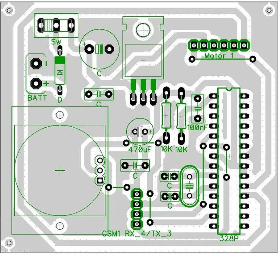
PCB layout
Before initiating a search for a 'pcb design company near me,' a precise understanding of your project's specific requirements is paramount. This includes defining the complexity of the design, the physical dimensions of the board, the materials to be used, and the intended functionality of the final product. A clearly defined set of requirements will serve as the foundation for selecting a suitable design partner and streamline the entire design process.
Project Complexity Determine whether your design is single-layer, multi-layer, analog, digital, or mixed-signal. This dictates the expertise required from a PCB design company.
Board Size and Shape Specify the precise dimensions and any specific form factors of your PCB. This impacts layout and routing considerations.
Material Selection Choose the right substrate based on your project's requirements for temperature, mechanical stress, and frequency. Common options include FR-4, Rogers, and others.
Functionality Clearly define all required functional aspects of the board including signal types, voltage levels, current requirements, connectivity needs, and compliance with any relevant standards.
Key Factors to Consider When Choosing a PCB Design Company
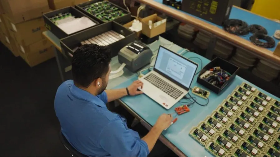
PCB design engineer
Selecting the right PCB design company is crucial for the success of your electronics project. Beyond just proximity, several factors warrant careful consideration to ensure the chosen partner aligns with your specific requirements and delivers high-quality results.
These key factors can be broken down into several key areas:
Experience and Expertise Evaluate the company's track record and the team's expertise in PCB design. Look for experience with similar projects in terms of complexity, technologies used, and industry standards.
Industry Certifications Verify the company holds relevant industry certifications (e.g., ISO 9001, IPC standards). Certifications demonstrate a commitment to quality and adherence to established processes.
Design Tools and Software Ensure the company utilizes industry-standard PCB design software (e.g., Altium Designer, Cadence Allegro, KiCad). Compatibility with your existing tools and preferred workflows is essential for seamless integration.
Portfolio and Past Projects Carefully review the company's portfolio. Look for evidence of diverse projects, varying levels of complexity, and successful designs that meet client requirements. This provides tangible proof of capability.
Communication and Project Management Assess the company's communication style, project management practices, and their ability to provide regular updates. Clear communication and structured project management are essential for a smooth collaboration.
A structured approach to evaluating these factors will enable you to identify a PCB design company that not only has the technical skills but also aligns with your project goals and ensures a successful outcome.
Local vs. Remote PCB Design Companies: A Comparative Analysis
Local PCB company
The decision between a local and remote PCB design company involves weighing several factors, primarily centered around communication, accessibility, and project management. While a 'pcb design company near me' offers the appeal of face-to-face interaction, remote options can provide access to specialized expertise and potentially lower costs. This section delves into a comparative analysis to help you make the optimal choice for your project.
Factor
Local PCB Design Company
Remote PCB Design Company
Communication
Direct face-to-face meetings possible; immediate feedback during crucial phases.
Primarily through digital channels (email, video calls); potential for delays in feedback.
On-Site Visits
Ease of visiting the facility for progress checks, audits and to meet with the team.
Site visits are not normally possible or will incur extra travel cost
Cultural Alignment
Reduced risk of cultural barriers; easier to establish a relationship with local staff.
Potential cultural differences might impact communication and project flow.
Response Time
Potentially quicker response times due to proximity and time zone alignment.
Possible delays due to time zone differences; may require flexible scheduling.
Cost
May have slightly higher costs due to local operational expenses and labor.
Often offers lower costs due to reduced overheads and access to global talent.
Expertise
May be limited by the local pool of resources; may require an extensive search.
Access to a global talent pool, specializing in specific aspects of PCB design.
Relationship Building
Greater opportunity to establish a long term business relationship
Less personal engagement and more transactional relationship
Ultimately, the selection between local and remote firms depends on your project's unique requirements. If rapid communication and the ability to meet in person are paramount, a local company might be the right fit. If you prioritize specialized expertise, cost efficiency and flexibility with location, a remote team should be considered. Thoroughly evaluate your needs before making a final decision to ensure project success.
The PCB Design Process: What to Expect
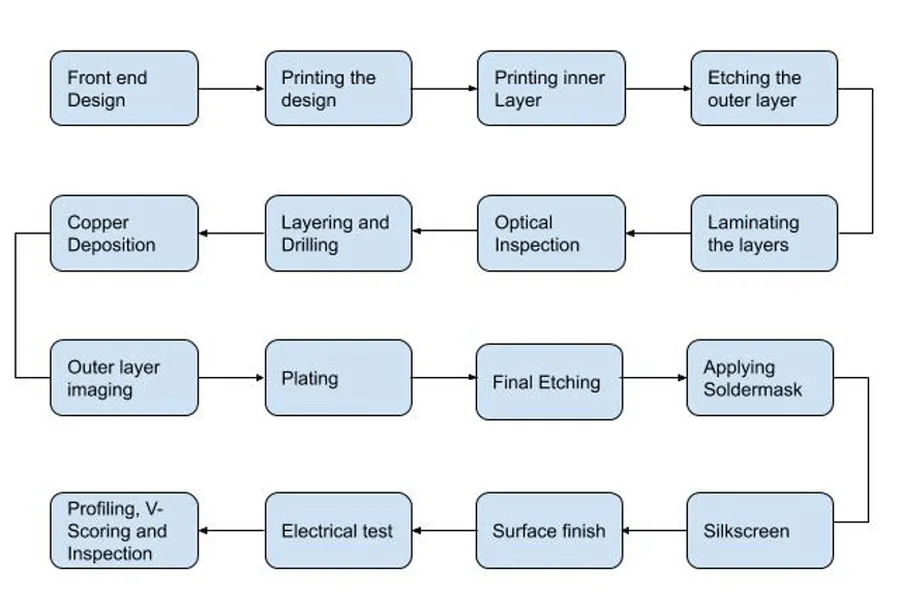
PCB design process
A typical PCB design process, managed by a 'pcb design company near me', involves a series of well-defined stages, from initial concept to final production. Understanding these steps will help you effectively collaborate with your chosen company and manage expectations for project timelines and deliverables.
Schematic Capture The process begins with translating your project's electrical specifications into a schematic diagram. This involves selecting electronic components and defining their interconnections using specialized CAD software. This stage is critical for establishing the functional blueprint of the PCB.
PCB Layout Design Once the schematic is complete, the physical layout of the PCB is created. This includes placing components onto the board and routing the electrical connections through copper traces. Considerations such as thermal management, signal integrity, and manufacturability are taken into account during this stage.
Design Rule Check (DRC) and Verification After layout, the design undergoes a Design Rule Check (DRC) to identify potential issues such as trace clearances and component overlaps, ensuring the board is electrically sound and producible. Further verification and simulation are often performed to ensure signal integrity, power delivery, and overall functionality.
Prototype Fabrication and Assembly The Gerber files created from the layout are sent to a PCB fabrication facility to produce a prototype board. Components are then assembled onto this board. This stage provides the first physical test of the design's functional performance.
Prototype Testing and Validation The assembled prototype undergoes thorough testing to verify its performance against the initial specifications and confirm functionality. Feedback from these tests is used to refine the design if necessary and improve overall reliability.
Production and Manufacturing Once the design has been thoroughly validated, it is released for mass production. The PCB fabrication and assembly are conducted based on the finalized design files. The 'pcb design company near me' may also manage sourcing of components and quality control during this phase.
Frequently Asked Questions About PCB Design Services
Navigating the world of PCB design can raise numerous questions. This section addresses the most common inquiries regarding PCB design services, helping you make informed decisions for your project.
How much does it cost to get a PCB assembled? The cost of PCB assembly varies significantly based on several factors, including the complexity of the design, the number of layers, the component count, the type of components (SMT vs. through-hole), the quantity of boards, and the turnaround time. Simple boards with fewer components and standard materials will cost less than complex, multilayer boards with specialized components. It is crucial to obtain quotes from multiple assembly houses to compare pricing and services.
How much should I charge for PCB design services? The rate for PCB design services can vary based on experience level, the complexity of the design, and the region. Entry-level designers may charge lower hourly rates, while experienced designers with expertise in specific areas (e.g., high-speed design, RF circuits) can command higher fees. Pricing models can be hourly, per-project, or even a combination thereof. To accurately determine your rates, consider your skill set, experience, overhead costs, and market demand.
Do electrical engineers design PCBs? While electrical engineers (EEs) are often involved in the overall design of electronic products, including circuit design and component selection, the actual physical layout of a printed circuit board (PCB) is frequently performed by PCB designers or layout engineers. Some EEs may have expertise in PCB design, particularly if they work in smaller organizations where roles are not strictly compartmentalized, but it is a specialized skill requiring specific training, experience with CAD tools, and an understanding of design rules for manufacturing.
What is the typical turnaround time for PCB design services? The turnaround time for PCB design is highly dependent on design complexity. Simple, single or double-layer boards with few components can be designed in a matter of a day or two. Complex, multi-layer boards with specific routing requirements, can take a week or more. Additionally, turnaround times are also affected by the availability and workload of the chosen design company. It is best to clarify timelines in advance with your chosen PCB design partner and factor in buffer time.
What software do PCB designers typically use? Professional PCB design relies on Electronic Design Automation (EDA) software suites. Popular choices include Altium Designer, Cadence Allegro, Mentor Graphics PADS, and KiCad (open-source). Each software package has its unique strengths, and the choice may depend on the designer's expertise, budget, and project requirements. Ensuring compatibility between the design company's software and your in-house systems is important if you intend to perform ongoing work or modify the design later.
What are the key elements of a high-quality PCB design? High-quality PCB design ensures functionality and reliability. Key elements include proper component placement and orientation, following design rules for manufacturability (DFM), impedance matching, thermal management, signal integrity, and minimizing electromagnetic interference (EMI). These considerations affect the performance, manufacturability, and longevity of the final product. A professional PCB design company will address these factors during the design process.
How can I ensure my PCB design is cost-effective? Cost-effective PCB design involves carefully considering the balance between performance and cost without sacrificing quality. Strategies include: minimizing the number of layers, selecting standard components, optimizing the board size, using efficient routing practices, and designing for manufacturability (DFM) to reduce assembly costs. Working closely with a design partner, and choosing the appropriate component types can contribute significantly to minimizing overall costs.
How to Evaluate PCB Design Company Portfolios
PCB Portfolio
Evaluating a PCB design company's portfolio is critical to ensure they have the expertise to meet your specific project requirements. A thorough review will reveal the breadth of their experience, the complexity of designs they’ve handled, and the overall quality of their work. This process helps in making an informed decision about the most suitable 'pcb design company near me' for your needs.
Diversity of Projects Look for a range of PCB designs across different industries and applications. This demonstrates adaptability and a wide skillset.
Complexity of Designs Assess the intricacy of their past projects. Can they handle multi-layer boards, high-density interconnects, or specialized materials if your project requires it?
Quality of Layout Examine the precision and detail of their layout work. This is crucial for signal integrity and overall performance of the PCB.
Similar Projects Prioritize portfolios with projects similar to your own. This will indicate their direct experience with the specific challenges and requirements of your design.
Industry Alignment Verify if the portfolio includes projects relevant to your industry vertical. Expertise in similar fields is a strong indicator of their capability to deliver a successful project for you.
Client Testimonials A good portfolio will often include client testimonials. These insights can provide a more comprehensive picture of the company's work quality and reliability.
Portfolio Aspect
Evaluation Criteria
What to look for
Diversity
Range of applications and industries
Broad experience, adaptable skill set
Complexity
Intricacy of designs
Ability to handle multi-layer, high-density, and specialized designs
Layout Quality
Precision and detail of layout work
Attention to signal integrity and overall performance
Project Similarity
Relevance to your project needs
Experience with designs similar to your requirements
Industry Alignment
Relevance to your vertical
Demonstrated expertise in your specific industry
Client Testimonials
Feedback from previous clients
Positive feedback regarding quality and reliability
Comparing PCB Design Software and Tools
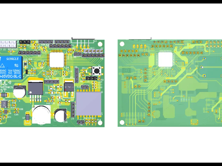
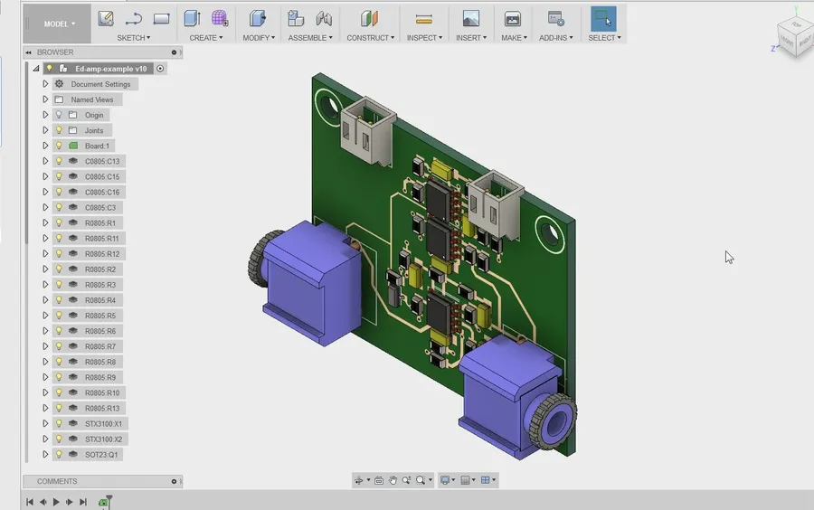
PCB Design software
The selection of PCB design software is a critical decision that significantly impacts project outcomes. Different software packages offer varying capabilities, user interfaces, and specialized features. Choosing software compatible with your project's requirements and the design company's workflow is essential for efficient and accurate PCB design.
Software
Description
Key Features
Typical Use Cases
Cost
Altium Designer
A comprehensive, high-end PCB design suite.
Advanced routing, signal integrity analysis, 3D visualization, and extensive component library.
Complex, multilayer PCBs, high-speed designs, and intricate layouts.
High
Cadence Allegro
A powerful software used for high-speed PCB design.
Robust constraint management, advanced routing capabilities, and signal integrity analysis tools.
High-speed digital designs, complex multilayer boards, and RF/microwave applications.
High
KiCad
An open-source, cross-platform PCB design suite.
Schematic capture, PCB layout, 3D viewer, and gerber file generation. Suitable for hobbyists and professionals.
Low to medium complexity designs, ideal for rapid prototyping and learning.
Free
Eagle (Autodesk EAGLE)
A popular PCB design software with a user-friendly interface.
Schematic capture, PCB layout, library management, and various routing options.
Small to medium complexity boards, suitable for a variety of applications from hobby projects to professional designs.
Medium
OrCAD
A widely used PCB design software with extensive features.
Schematic capture, PCB layout, simulation, and analysis tools.
Medium to high complexity designs, suitable for various electronic applications.
Medium to High
PADS (Siemens PADS)
A complete design and analysis environment for PCB design.
Advanced routing, signal integrity analysis, thermal analysis, and manufacturing integration.
Complex PCBs, high-speed designs, and critical applications requiring simulation and analysis.
High
When evaluating a 'pcb design company near me,' inquire about the specific software and tools they use and ensure it aligns with your project's requirements, including file compatibility, feature needs, and industry standards. This ensures seamless collaboration and efficient project execution.
Cost-Effective PCB Design Solutions
Achieving cost-effective PCB design involves a multi-faceted approach, focusing on design optimization for manufacturability (DFM), strategic component selection, and smart vendor selection when searching for a 'pcb design company near me'. By addressing these areas, you can significantly reduce production costs without compromising quality or performance.
Design for Manufacturability (DFM) Implement DFM principles early in the design phase, this reduces manufacturing costs by optimizing layout for automated assembly, this will minimizes assembly time, materials, and potential errors.
Component Selection Opt for standard, readily available components over specialized parts. Evaluate the total cost of ownership including purchasing, manufacturing, and sourcing of components, not only component prices. The cost will be lower due to volume discounts, standard components are typically lower cost compared to specialized ones, and reduces lead times.
Panelization When designing multiple PCBs, consider panelization, which involves grouping several boards on a single larger panel. This will enable cost savings by reducing material waste and streamlining the manufacturing process.
Layer Count Carefully determine the necessary layer count. Adding more layers increases complexity and cost. Aim to use the minimum layers possible while fulfilling your design requirements. An appropriate layer count helps to reduce costs without sacrificing performance.
Vendor Negotiation and Bidding When looking for a 'pcb design company near me', obtain quotes from multiple providers. Negotiate prices based on your volume, and be prepared to discuss material and specification options to achieve the most cost-effective solution. Clear communication of your budget can lead to cost-saving alternatives from PCB vendors.
Cost Reduction Strategies
Description
Impact
DFM Optimization
Designing the PCB for efficient manufacturing.
Reduces assembly time and costs.
Standard Component Selection
Choosing readily available components.
Decreases component costs and lead times.
Panelization
Designing multiple PCB boards on a single larger panel.
Reduces material waste and manufacturing costs
Layer Count Optimization
Using the necessary layers for functionality.
Lowers the cost of materials, and can help streamline manufacturing process.
Vendor Negotiation
Obtaining multiple quotes.
Reduces pricing and lead to cost-saving options
Ensuring Quality and Reliability in PCB Design
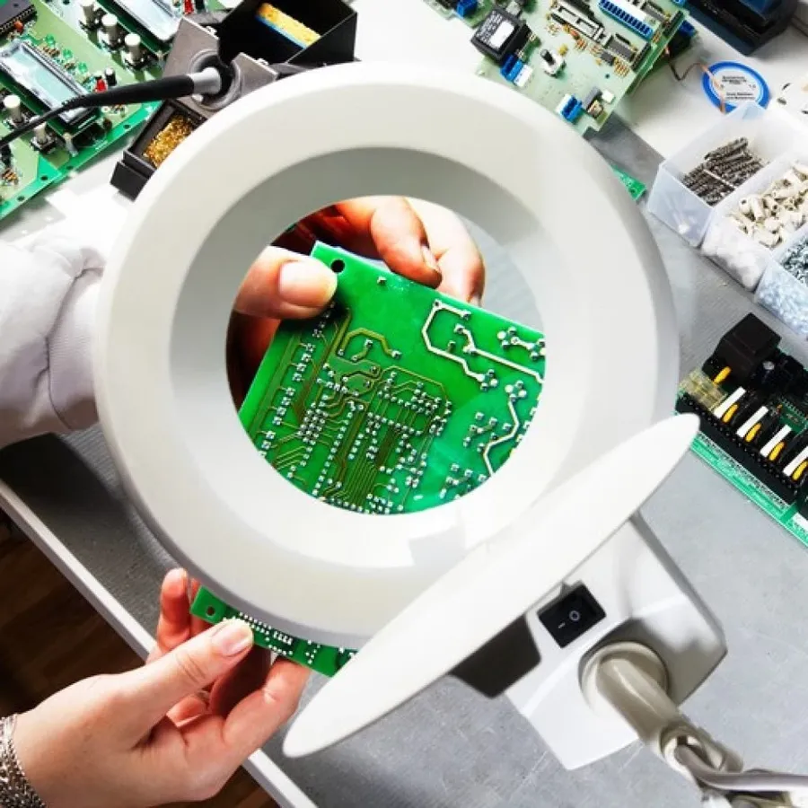
PCB Inspection
Quality and reliability are paramount in PCB design, directly impacting the functionality and lifespan of electronic devices. Adhering to stringent design rules and implementing comprehensive testing protocols are crucial steps to ensure the final product meets the required standards and performs as intended. A robust approach to quality control minimizes risks of failure and enhances overall product reliability.
Importance of Adhering to Design Rules Strictly following established design rules and guidelines is critical to prevent manufacturing issues, ensure signal integrity, and minimize electromagnetic interference (EMI). These rules address aspects like trace width, spacing, via placement, and component clearance, all of which affect performance and reliability.
Comprehensive Testing Protocols Rigorous testing, including functional testing, in-circuit testing (ICT), and boundary scan testing, ensures that the designed PCB operates correctly under various conditions. These tests verify signal paths, component functionality, and the overall integrity of the board.
Quality Control Processes A well-defined quality control process is essential, encompassing detailed inspections at different stages of production. This includes visual checks, X-ray inspections, and automated optical inspections (AOI), designed to detect any defects or deviations from the design specifications. Continuous process monitoring helps maintain high quality outputs.
Industry Certifications Working with a PCB design company holding relevant certifications like ISO 9001 demonstrates a commitment to quality management systems and processes. Compliance with industry standards, like IPC standards, ensures reliability and consistency in the manufacturing process. These certifications are often good indicators of a company’s quality focus.
Finding the right 'pcb design company near me' is a crucial step in bringing your electronic project to life. By carefully considering your specific needs, evaluating potential partners, and asking the right questions, you can ensure a successful outcome, and partnering with the right team will lead to high-quality, reliable, and cost-effective PCB solutions that meet your objectives. Keep exploring and remember the best partner is the one that best aligns with your vision and has the knowledge to get you there.