
As the global transition to electric mobility accelerates, the demand for power inverters that can handle higher currents without catastrophic thermal failure has reached a breaking point. Conventional printed circuit boards are struggling to meet the performance benchmarks of next-generation EV platforms. Enter heavy copper technology: a robust, high-performance solution that is effectively redefining the thermal and electrical limitations of modern automotive drive units.
The Evolution of Power Electronics in EVs
The Shift Toward High-Performance Power Conversion
In the nascent stages of electric vehicle development, power electronics were largely focused on auxiliary systems and low-voltage traction motors. Today, the demands of next-generation EVs—driven by 800V architectures and ultra-fast charging capabilities—have forced a complete architectural rethink. The modern power inverter must handle significantly higher currents while maintaining peak efficiency in a compact, lightweight footprint. This evolution has pushed traditional standard FR4 PCBs to their physical and thermal limits, making the integration of heavy copper technology a prerequisite for high-performance powertrain reliability.
Performance Comparison: Standard vs. Heavy Copper
| Feature | Standard PCB (1-2 oz) | Heavy Copper PCB (>3 oz) |
|---|---|---|
| Current Carrying Capacity | Limited; prone to trace heating | High; supports intense power density |
| Thermal Dissipation | Requires external cooling hardware | Integrated; acts as a structural heat sink |
| Mechanical Robustness | Vulnerable to vibration fatigue | High; provides structural integrity |
| Application Focus | Low-voltage logic and signaling | Power modules and motor inverters |
Key Challenges in Modern Inverter Design
- Why is thermal management critical in 800V systems?
As voltage and switching frequencies increase to reduce charging times, heat generation at the semiconductor interface rises exponentially, requiring low-impedance paths that only heavy copper can provide. - How does PCB thickness impact inverter size?
By utilizing thicker copper layers, engineers can eliminate the need for redundant busbars and external wiring harnesses, allowing for a more compact and integrated power module design. - What role does copper weight play in long-term reliability?
Increased copper weight significantly lowers electrical resistance, reducing ohmic heating and preventing the thermal cycling failures that frequently occur in overstressed standard PCBs.
Understanding Heavy Copper PCB Technology
Defining Heavy Copper Architecture
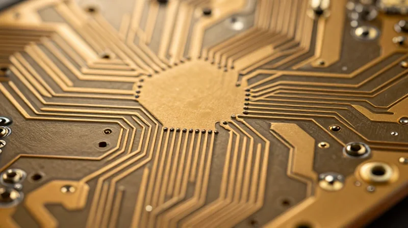
Heavy copper PCB technology is defined by the use of copper weights exceeding 3 ounces (oz) per square foot, with industrial-grade applications often scaling up to 10 oz or more. Unlike standard printed circuit boards, which typically employ 0.5 oz to 2 oz of copper, heavy copper variants feature thicker cross-sectional areas. This structural enhancement allows the board to sustain higher current flows without excessive thermal buildup, making them indispensable for the high-power density required by modern electric vehicle inverter systems.
Technical Comparison: Standard vs. Heavy Copper
| Feature | Standard PCB | Heavy Copper PCB |
|---|---|---|
| Copper Thickness | 0.5 oz - 2 oz | 3 oz - 10+ oz |
| Current Capacity | Moderate | Very High |
| Thermal Management | Basic | Excellent (Heat dissipation) |
| Primary Use Case | Logic & Signal | Power Electronics/Inverters |
Why EVs Require Heavy Copper
The transition to 800V architectures in next-gen electric vehicles places unprecedented stress on power electronics. Standard PCB traces would suffer from resistive heating, leading to board delamination or outright failure under sustained high-current operation. Heavy copper technology mitigates these risks by reducing electrical resistance, effectively serving as an integrated heat sink that channels thermal energy away from sensitive components.
- How does copper thickness affect current?
Electrical resistance is inversely proportional to the cross-sectional area of the conductor; increasing copper thickness drastically lowers resistance, allowing more current to pass while generating less heat. - Is heavy copper board production complex?
Yes, etching thick copper requires specialized chemical processes and precision manufacturing techniques to ensure trace integrity and minimize undercutting. - Does heavy copper impact component footprint?
While trace widths can sometimes be reduced due to the increased thickness, the manufacturing requirements generally necessitate design considerations regarding board stack-up and thermal relief pads.
Addressing Thermal Efficiency Constraints

Thermal Conductivity as a Design Constraint
In next-generation power inverters, thermal dissipation is the primary limiting factor for power density. Standard PCBs, typically utilizing 1 oz (35 µm) copper weight, often fail to conduct the significant heat generated by high-switching-frequency MOSFETs and IGBTs. Heavy copper PCBs, defined by copper weights ranging from 3 oz to 20 oz or more, act as functional heat sinks that distribute thermal energy across the substrate more effectively, preventing localized hot spots that lead to component degradation and premature failure.
Comparison of Thermal Performance
| Feature | Standard PCB (1 oz) | Heavy Copper PCB (≥3 oz) |
|---|---|---|
| Thermal Resistance | High | Low |
| Heat Spreading | Localized | Excellent/Global |
| Thermal Mass | Minimal | Significant |
| Mechanical Stress | Moderate | Reduced via Rigidity |
Mitigating Mechanical Stress Through Substrate Rigidity
Beyond thermal conductivity, the mechanical profile of heavy copper plays a critical role in system reliability. EV inverters are subject to extreme vibration and thermal cycling. The increased cross-sectional area of copper traces improves the structural integrity of the PCB, reducing board flex under thermal expansion. This reduction in mechanical stress directly mitigates the risk of micro-cracking in solder joints and through-hole vias, which are common failure points in high-power automotive electronics.
Thermal Efficiency FAQ
- How does heavy copper reduce the need for external heat sinks?
By increasing the copper volume, the PCB itself gains a higher thermal mass, allowing it to absorb and spread heat away from power semiconductors, effectively reducing the dependency on bulky external cooling solutions. - Does heavy copper impact the board's structural reliability under vibration?
Yes, the increased copper mass contributes to the overall rigidity of the board, minimizing PCB deflection and lowering the mechanical fatigue experienced by surface-mounted power components during vehicle operation. - Is there a trade-off in fabrication complexity?
While heavy copper requires specialized etching processes and longer manufacturing times, the long-term reliability gains and thermal performance outweigh the initial complexity in high-voltage inverter applications.
Comparison: Heavy Copper vs. Traditional PCBs
Comparative Performance Analysis
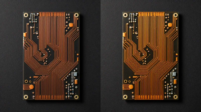
While standard PCBs are sufficient for signal processing and low-power control circuitry, they fail under the high-current demands of modern electric vehicle power inverters. Heavy copper PCBs (typically defined as 3 oz/ft² or greater) provide a significantly lower impedance path, which is essential for minimizing resistive losses, heat generation, and voltage drops during high-acceleration or rapid-charging scenarios.
| Feature | Standard PCB | Heavy Copper PCB |
|---|---|---|
| Copper Thickness | 0.5 - 2 oz | 3 - 20+ oz |
| Current Capacity | Low to Moderate | Extremely High |
| Thermal Dissipation | Relies on external sinks | Integrated heat dissipation |
| Mechanical Stress | Susceptible to warping | High structural integrity |
| Failure Risk | High at peak loads | Minimal due to redundancy |
Key Performance Metrics in Automotive Environments
Automotive environments demand components that can withstand extreme temperature cycling without fatigue. Standard PCBs often suffer from micro-cracking at the copper-substrate interface during rapid thermal expansion. In contrast, the thicker copper cross-section in heavy copper designs distributes thermal energy more uniformly, effectively dampening the mechanical stress exerted on solder joints and component interconnects.
- Does heavy copper increase physical board weight?
Yes, it contributes to overall mass, but in the context of EV inverters, the weight penalty is offset by the ability to downsize auxiliary cooling systems, leading to a net gain in system-level efficiency. - How does current density differ between the two?
Heavy copper reduces the required trace width for high-current paths, allowing for more compact designs that maintain low operating temperatures even when carrying hundreds of amperes. - Are heavy copper PCBs more reliable long-term?
Absolutely; they offer superior resistance to environmental degradation and electrical surges, which is critical for the long-lifecycle requirements of automotive power electronics.
Driving High Power Density in Traction Inverters
Driving High Power Density in Traction Inverters
The evolution of electric vehicle (EV) traction inverters is defined by the relentless pursuit of power density. As automotive engineers strive to shrink the footprint of power electronics without sacrificing performance, the integration of heavy copper PCB technology has emerged as a critical design enabler. Unlike standard PCBs, which often require auxiliary busbars and additional thermal management components, heavy copper traces serve a dual purpose: conducting massive current loads and acting as an integrated heat-dissipation substrate.
Optimizing Space through Integrated Power Distribution
By utilizing heavy copper (typically defined as 3 oz/ft² or greater), designers can drastically reduce the physical volume of the power stage. High-current traces can be routed directly on the PCB, replacing bulky external cabling and mechanical connectors that traditionally consumed valuable chassis space. This consolidation directly translates into smaller, lighter, and more aerodynamically efficient traction drive units.
| Feature | Standard PCB | Heavy Copper PCB |
|---|---|---|
| Component Count | High (requires busbars/extra heatsinks) | Low (integrated thermal path) |
| Power Density | Moderate | Ultra-High |
| Thermal Impedance | High | Low |
| System Volume | Larger | Compact |
Frequently Asked Questions on Power Density
- How does heavy copper reduce total system weight?
By eliminating the need for external copper busbars, heavy-duty connectors, and separate cooling plates, heavy copper PCBs consolidate power paths directly onto the board, significantly trimming the system's overall mass. - Is heavy copper compatible with high-frequency switching?
Yes, although trace geometry must be carefully managed to mitigate skin effect losses. When designed correctly, the low resistance of heavy copper helps maintain signal integrity while handling high-current transients essential for modern SiC-based inverters. - What is the primary trade-off in space-constrained designs?
The main challenge is balancing the increased trace width required for high current with the desire for component density; however, advanced multi-layer heavy copper stackups effectively manage this by distributing load across parallel planes.
Material Science and Manufacturing Challenges

Advanced Etching and Fabricating Challenges
The primary manufacturing challenge with heavy copper—defined as copper weights exceeding 3 oz/ft²—lies in the geometry of the traces. Standard chemical etching processes often lead to 'undercutting,' where the etchant erodes the copper beneath the photoresist, resulting in non-uniform, trapezoidal trace profiles. Achieving near-vertical sidewalls is critical in automotive power electronics to maintain consistent impedance and current distribution. Fabricators must employ multi-step etching sequences, specialized acid chemistries, and precise mask compensation to ensure structural integrity and prevent stress concentration points.
Soldering and Assembly Complexities
Assembly introduces a secondary layer of complexity: thermal mass. Heavy copper layers act as massive heat sinks, which rapidly dissipate energy during the reflow process. This makes reaching the liquidus temperature of standard lead-free solders (like SAC305) difficult without damaging surface-mount components through prolonged heat exposure. To mitigate this, manufacturers must utilize high-capacity forced convection reflow ovens and, in some cases, localized laser or induction soldering to ensure robust intermetallic compound formation without compromising the substrate.
| Parameter | Standard PCB (0.5-1 oz) | Heavy Copper PCB (>3 oz) |
|---|---|---|
| Etching Technique | Single-stage chemical | Multi-stage with pulse etching |
| Reflow Heat Capacity | Low thermal mass | High thermal mass |
| Trace Profile | Standard side-wall | Requires vertical edge control |
| Reliability Risk | Surface delamination | Solder joint thermal fatigue |
Manufacturing FAQ
- Why is undercut a critical failure point in heavy copper?
Excessive undercut creates narrow trace bases, which increases local current density and causes localized overheating, potentially leading to trace separation under thermal cycling. - How does heavy copper affect substrate selection?
The high coefficient of thermal expansion (CTE) mismatch between thick copper and the base laminate (typically FR-4) requires high-Tg or ceramic-filled materials to prevent board warpage and via cracking. - Is standard AOI (Automated Optical Inspection) sufficient?
Standard AOI struggles with the steep vertical profile of heavy copper. 3D-AOI is generally required to accurately verify trace width and height tolerances.
Long-Term Reliability and Automotive Standards
Compliance with Automotive Safety Standards
The transition to 800V architectures in next-gen EVs demands components that surpass standard reliability benchmarks. Heavy copper PCBs contribute to compliance with IATF 16949 and ISO 26262 by mitigating the risks of thermal degradation, which is a common failure mode in traction inverter power stages. By reducing trace resistance, these boards lower operating temperatures, thereby extending the mean time between failures (MTBF) and meeting stringent safety integrity level (ASIL) requirements.
Comparative Reliability Metrics
| Parameter | Standard PCB | Heavy Copper PCB |
|---|---|---|
| Thermal Cycling Resilience | Moderate (risk of trace cracking) | High (superior CTE matching) |
| Current Overload Capacity | Limited (potential for delamination) | Excellent (high thermal dissipation) |
| Vibration/Shock Resistance | Standard | Enhanced (structural rigidity) |
Frequently Asked Questions
- How does heavy copper aid in ISO 26262 certification?
Heavy copper reduces localized heating, which prevents intermittent signal faults and catastrophic short-circuit failures, providing a more stable physical layer for safety-critical hardware. - Do heavy copper boards perform better under long-term vibration?
Yes, the increased copper mass provides additional structural reinforcement to the PCB substrate, significantly improving the fatigue life of solder joints in high-vibration automotive environments. - Is the reliability cost-effective for mass-market EVs?
While manufacturing costs are higher, the reduction in warranty claims and field failures related to power module overheating makes it the preferred choice for long-cycle automotive platforms.
The Future Trajectory of EV Power Design
The Synergy of Wide-Bandgap Semiconductors and Heavy Copper
As Silicon Carbide (SiC) and Gallium Nitride (GaN) become the standard for power inverters, the thermal management demands shift significantly. While these semiconductors enable faster switching frequencies and reduced switching losses, they also concentrate heat in smaller footprints. Heavy copper PCBs act as a structural heat sink, directly addressing these thermal bottlenecks by providing a low-resistance path for heat dissipation that standard PCBs simply cannot support.
| Feature | Standard PCB Integration | Heavy Copper Synergy |
|---|---|---|
| Switching Frequency | Moderate (Limits efficiency) | High (Stable thermal control) |
| Thermal Conductivity | Substrate-dependent | Enhanced via copper mass |
| Current Density | Low (Requires large footprint) | High (Optimized, compact design) |
Predicting Future Industry Trends
Future power design will move toward 'embedded power' modules where semiconductors are integrated directly within the PCB stack-up. This shift will require heavy copper to act as both an electrical conductor and a structural component for EMI shielding, effectively creating a multi-functional power delivery network that simplifies the assembly of high-power automotive systems.
Frequently Asked Questions on Future EV Power Design
- Will heavy copper replace thermal interface materials (TIM)?
Heavy copper reduces the reliance on bulky TIM by distributing heat more effectively across the board surface, though it will likely function alongside high-performance gap pads for the foreseeable future. - How does GaN adoption impact PCB trace requirements?
GaN's extremely high switching speed requires lower loop inductance, which is better achieved through the rigid and thick trace geometries inherent in heavy copper manufacturing. - Is the transition to heavy copper cost-prohibitive for mass-market EVs?
While unit costs are higher, the overall system-level savings achieved through reduced cooling requirements and smaller inverter sizes make it a net-positive investment for long-range EV platforms.
Heavy copper technology is not merely an improvement on standard PCB manufacturing; it is a fundamental shift toward the high-current, high-efficiency architectures that define the future of automotive electrification. By optimizing thermal management and power density today, manufacturers can secure a competitive edge in tomorrow's market. Contact our engineering team today to discuss how our heavy copper solutions can optimize your next-gen EV inverter project.
