
As power density demands in automotive inverters continue to climb, traditional PCB fabrication methods are being pushed to their breaking point. To achieve high current capacity without sacrificing reliability, design engineers must master the nuances of heavy copper manufacturing. This guide provides the critical Design for Manufacturing (DFM) framework needed to balance high-amperage performance with board-level manufacturability.
The Physics of Heavy Copper: Understanding Impedance and Heat
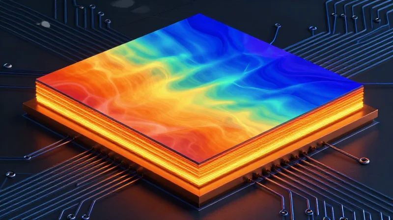
The Relationship Between Copper Cross-Section and Impedance
In high-current power electronics, the primary function of heavy copper (typically defined as copper weights exceeding 3 oz/ft²) is to minimize ohmic losses. Electrical resistance in a conductor is inversely proportional to its cross-sectional area. By increasing the copper thickness, you effectively increase the conductive path, which significantly lowers the DC resistance ($R = ho L/A$). Lowering this resistance is critical for inverters, as it minimizes the voltage drop ($V=IR$) and drastically reduces power dissipation ($P=I^2R$), preventing excessive heat generation at the board level.
Thermal Management and Heat Dissipation
Heavy copper acts as an integrated heat sink. Because copper has excellent thermal conductivity, thicker layers allow heat generated by power MOSFETs or IGBTs to spread laterally across the board surface more efficiently. This reduces local thermal stress (hot spots) and lowers the junction-to-ambient thermal resistance ($ heta_{JA}$). For inverter designers, this means improved reliability and the ability to operate at higher power densities without immediate failure.
| Copper Weight (oz) | Approx. Thickness (mm) | Thermal Advantage |
|---|---|---|
| 1 oz | 0.035 mm | Baseline/High Resistance |
| 3 oz | 0.105 mm | Moderate Heat Spreading |
| 6 oz | 0.210 mm | Superior Power Handling |
Frequently Asked Questions
- Why not just make traces wider instead of thicker?
While widening traces also increases cross-sectional area, it consumes precious PCB real estate. Heavy copper allows for high-current capacity in a compact footprint, essential for space-constrained inverter modules. - Does heavy copper affect thermal expansion?
Yes. The increased mass of copper creates a larger coefficient of thermal expansion (CTE) mismatch with the FR-4 substrate, which can lead to barrel cracking in vias if proper DFM guidelines regarding aspect ratios and plating thickness are not followed.
Strategic Trace Spacing and Aspect Ratios
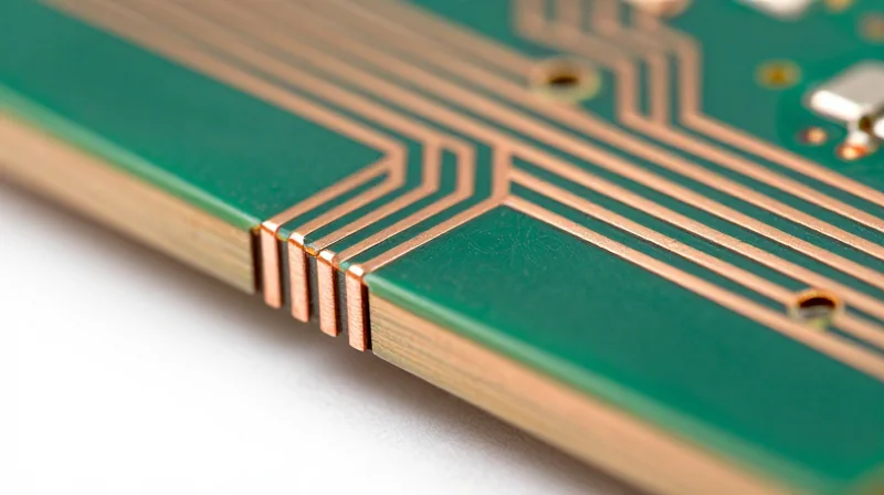
The Challenge of Etching High-Copper Volumes
In heavy copper PCBs (typically 3 oz to 30 oz copper), maintaining consistent trace spacing is significantly more complex than in standard 1 oz designs. Because heavy copper requires longer immersion in etching chemicals, the chemical process tends to 'undercut' the sides of the traces. This results in a trapezoidal cross-section rather than a perfectly rectangular one. To prevent electrical shorts and maintain signal integrity, designers must increase minimum spacing beyond standard PCB guidelines to compensate for this lateral etching.
Aspect Ratios and Etch Factor
The aspect ratio—defined as the ratio of trace height to base width—is a crucial DFM metric. As copper thickness increases, the etch factor must be accounted for to ensure the base width of the conductor remains within tolerance. Failing to respect the etch factor leads to 'bridge' shorts between closely spaced traces, especially in dense inverter power stages.
| Copper Weight (oz) | Min. Trace Spacing (mm) | Recommended Etch Allowance |
|---|---|---|
| 2 oz | 0.20 mm | Low |
| 4 oz | 0.40 mm | Moderate |
| 6 oz+ | 0.75 mm+ | High |
DFM Best Practices for Trace Layout
- How does heavy copper affect lateral etching?
Longer etch cycles required to remove thick copper result in significant lateral erosion of the trace sidewalls, necessitating wider air gaps to avoid shorts. - What is the rule of thumb for clearance?
A general rule is to maintain a spacing-to-thickness ratio of at least 1:1, though this should be verified with your specific fabricator’s chemical etch capabilities. - Why is the aspect ratio important for inverters?
High aspect ratios in power traces can lead to resistive heating concentration at the base of the trace, potentially causing localized delamination or failure under sustained high-current loads.
Advanced Etching Compensation Techniques
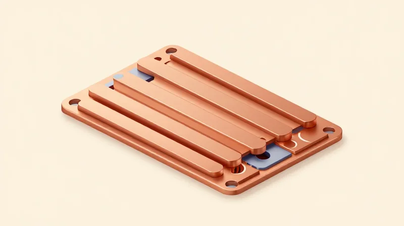
In heavy copper designs (3oz and above), standard chemical etching processes consume copper not just from the surface, but horizontally along the sidewalls, resulting in an undercut. To maintain the precise trace width required for high-current inverter performance, engineers must proactively adjust their Gerber files by oversizing tracks during the design phase.
Quantifying the Etch Factor
The etch factor is the ratio of depth etched to the lateral side-etching distance. As copper thickness increases, the duration of the etch bath must extend, leading to more significant width reduction. If the trace is not compensated, final impedance and current-carrying capacity will deviate significantly from your simulation results.
| Copper Weight (oz) | Typical Etch Compensation (mil) | Impact on High-Current Design |
|---|---|---|
| 2 oz | 0.5 - 1.0 | Negligible for most power traces |
| 3 - 4 oz | 1.5 - 2.5 | Essential for thermal dissipation |
| 6+ oz | 3.0 - 5.0 | Critical to prevent narrowing failures |
Best Practices for Gerber Compensation
- How do I calculate the specific compensation factor?
Consult your PCB fabricator for their specific 'etch factor' data, as this is highly dependent on their proprietary chemical line and conveyor speeds. - Does etching affect rounded vs. square corners differently?
Yes. Sharp 90-degree corners are prone to 'clipping' during prolonged etching; consider using rounded or tear-drop pads to ensure even chemical exposure and consistent trace width. - Should I apply compensation globally or locally?
Apply compensation locally to high-current tracks only. Applying global compensation to signal-layer traces (1oz or less) can cause impedance mismatches and spacing violations.
By implementing these DFM modifications, you ensure that the manufactured PCB matches the theoretical current capacity modeled in your design software. Always verify these offsets with your manufacturer's CAM engineer before finalizing fabrication data.
Optimizing Via Arrays for Thermal Dissipation
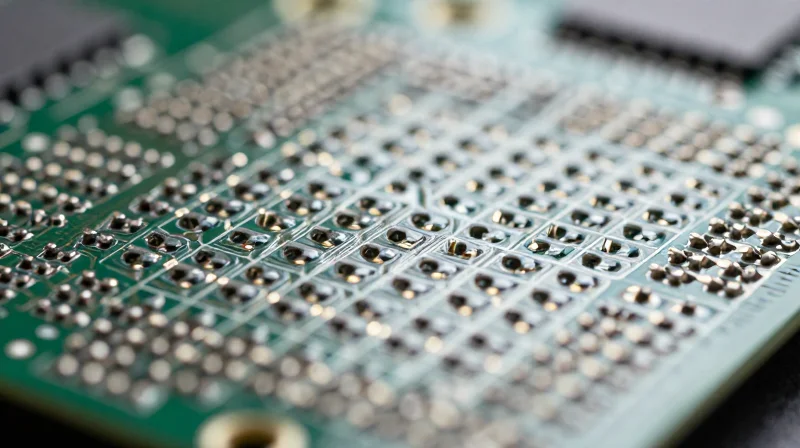
Thermal Via Strategy for Power Stages
In heavy copper designs, thermal vias act as critical conduits for transferring heat from power semiconductor junctions to the underlying heatsink or chassis. To maximize efficiency, place via arrays directly under the thermal pad of power components, utilizing a tight grid pattern to minimize thermal resistance. However, because heavy copper (3oz or greater) complicates chemical plating processes, engineers must balance thermal density with the risk of plating voids.
Plating Integrity and Void Prevention
The high aspect ratio of thick copper boards creates significant challenges for copper plating chemistry reaching the center of a via hole. Voids within these vias create insulation gaps that drastically reduce thermal performance and electrical reliability. To mitigate this, define larger drill diameters relative to the board thickness and ensure clear specifications for barrel plating thickness.
| Via Feature | Best Practice | Reasoning |
|---|---|---|
| Drill Diameter | 0.3mm to 0.4mm | Promotes better chemical flow/plating coverage. |
| Via Pitch | 1.0mm to 1.25mm | Balances copper mass with structural integrity. |
| Plugging Method | Conductive epoxy fill | Prevents solder wicking and increases conductivity. |
Frequently Asked Questions
- Should I cap my thermal vias with solder mask?
Avoid tenting vias with solder mask on the bottom side if they contact a heatsink, as the mask can act as an insulating thermal barrier; leave them open or use a thermally conductive plug. - Does copper weight affect via drill size?
Yes. Heavier copper restricts the aperture of the via after plating, so start with a larger drill diameter than you would for standard 1oz boards to ensure the required finished hole size is met. - Are filled vias necessary for high-current inverters?
Filled and capped (via-in-pad) designs are highly recommended to prevent solder from wicking away from the component pad during reflow, which ensures a superior mechanical and thermal bond.
Surface Finish Challenges for High-Current Joints
Surface Finish Reliability in High-Power Environments
In high-current inverter designs, the surface finish must do more than prevent oxidation; it must facilitate reliable solder joints that can withstand significant thermal expansion cycles. Unlike standard logic-level circuits, power joints experience substantial mechanical stress during thermal cycling, making the choice of finish a primary factor in preventing interfacial failure and fatigue cracks.
Comparative Analysis of Surface Finishes
| Finish Type | Thermal Reliability | Surface Flatness | Suitability for High Current |
|---|---|---|---|
| HASL (Leaded/Lead-Free) | Low (Brittle IMCs) | Poor (Uneven) | Not Recommended |
| ENIG | Moderate | Excellent | Limited by Gold Thickness |
| Immersion Silver (ImAg) | High | Excellent | High |
| ENEPIG | Highest | Excellent | Best |
Frequently Asked Questions
- Why is standard HASL unsuitable for heavy copper power components?
HASL provides an uneven surface that complicates the assembly of high-current power modules. Furthermore, the thickness variation often leads to non-planar solder joints, creating localized stress concentrations during thermal expansion. - Does the gold in ENIG cause brittleness in power joints?
Yes, if the gold layer is too thick, it can lead to gold-embrittlement of the solder joint. For power applications, strictly controlled, thin immersion gold is required to ensure the solder bonds directly to the nickel barrier layer. - Is Immersion Silver (ImAg) a viable alternative?
ImAg provides an excellent, flat surface that is highly conductive and free from gold-embrittlement risks. It is often favored in high-current designs, provided the environment is managed to minimize sulfur-based corrosion.
For designs requiring the highest level of reliability in rugged thermal environments, ENEPIG (Electroless Nickel Electroless Palladium Immersion Gold) is the professional standard. It provides a robust diffusion barrier, superior solderability, and resistance to the mechanical stresses inherent in high-current inverter operations.
Mitigating Delamination and CTE Mismatch

Managing CTE Mismatch in Heavy Copper Structures
Heavy copper PCBs (typically >3 oz) exert significant mechanical forces on the laminate during thermal transitions due to the difference in the Coefficient of Thermal Expansion (CTE) between the thick copper layers and the fiberglass-epoxy substrate. To prevent structural failure, designers must prioritize materials with a lower Z-axis CTE and higher glass transition temperature (Tg) to maintain bond strength and signal integrity.
| Parameter | Standard FR-4 | High-Tg/High-Performance Laminate |
|---|---|---|
| Glass Transition (Tg) | 130°C - 140°C | 170°C - 180°C+ |
| Z-Axis CTE | High (4.0 - 5.0%) | Low (<3.0%) |
| Thermal Reliability | Poor for power cycles | Excellent for power cycles |
Best Practices for Material Selection
- Prioritize High-Tg Materials
Select laminates with a Tg above 170°C to ensure the material remains in its rigid state despite the heat generated by high-current loads. - Balance Copper Distribution
Ensure symmetrical copper distribution across board layers to minimize mechanical warping and internal stress accumulation during reflow. - Specify Low-Flow Prepregs
Use low-flow or no-flow prepregs to prevent resin starvation in dense heavy copper areas, which reduces the risk of post-processing delamination.
Mitigating Delamination Risks
Delamination is frequently triggered by moisture absorption and inadequate bond strength between thick copper features and the resin matrix. Designers should mandate high-peel strength copper foils and ensure that the PCB fabrication process includes adequate bake-out procedures to remove entrapped moisture prior to high-temperature assembly. Furthermore, maintaining consistent trace spacing prevents localized resin-rich or resin-starved regions that compromise the board's structural integrity.
Validating Reliability: Power Cycling and Stress Testing
Validating Reliability: Power Cycling and Stress Testing
Ensuring the longevity of heavy copper PCBs requires rigorous validation beyond standard electrical continuity checks. In high-current inverter applications, the primary failure modes are driven by thermal expansion, cyclic fatigue, and interconnect degradation. Implementing structured stress testing ensures your PCB layout survives the cumulative damage of automotive-grade thermal profiles.
Core Reliability Testing Procedures
| Test Type | Target Metric | Purpose for Heavy Copper |
|---|---|---|
| Power Cycling | dT/dt Stress | Validates interconnect fatigue from copper/dielectric CTE mismatch. |
| Thermal Shock | Cycled Temp Extremes | Identifies potential delamination or crack initiation at heavy copper vias. |
| High-Current Endurance | Steady State Temp | Confirms trace thermal stability and solder joint creep resistance. |
Best Practices for Reliability Validation
- Implement Instrumented Test Coupons
Include daisy-chain patterns within your panel to monitor resistance increases in real-time during thermal cycling, allowing for early detection of crack initiation. - Monitor Interconnect Integrity
Utilize cross-sectional analysis post-stress to verify that copper plating in high-aspect-ratio holes has not separated from the internal layers. - Adhere to Automotive Standards
Align testing protocols with IPC-9701 and AEC-Q100/200 requirements to ensure consistent reporting across harsh operating environments.
Reliability is not merely about surviving the initial build; it is about maintaining performance over thousands of heating cycles. If your design shows resistance drift greater than 5% during accelerated life testing, revisit your stack-up to ensure better CTE matching and optimized copper distribution.
Collaboration with Fabricators: The DFM Review Process
The Proactive DFM Review Strategy
Collaboration must begin long before the final Gerber release. By involving fabrication engineers early, you can reconcile high-current design requirements with the mechanical capabilities of the shop floor. Heavy copper designs, particularly those with 3oz to 6oz+ copper, introduce significant challenges regarding etching tolerances, aspect ratios for vias, and thermal dissipation paths that standard PCB design rules may not adequately address.
Essential Pre-Fabrication Checklist
- Etch Factor Compensation
Confirm that the fabricator has accounted for heavy copper lateral etching. Ask how they adjust the artwork compensation to meet your final trace width requirements. - Stackup Symmetry
Review the proposed stackup with the vendor to ensure copper balance, which is critical for minimizing warpage during the high-heat lamination cycles required for heavy copper materials. - Via Filling Requirements
Clarify if the design requires conductive or non-conductive via fill. High-current designs often mandate specific fill materials to handle thermal expansion without cracking via barrels. - Surface Finish Compatibility
Discuss the impact of the chosen finish on high-power solder joint reliability, ensuring it supports the heavy-duty assembly processes characteristic of inverter production.
Communication Matrix: Design Intent vs. Fab Capability
| Design Parameter | Common Risk | Collaborative Action |
|---|---|---|
| Trace Widths | Under-etched signals | Provide min/max copper weight zones. |
| Via Plating | Barrel cracking | Request increased plating thickness (min 25µm). |
| Copper Pour | Board Bow/Twist | Define cross-hatching or balanced fill areas. |
Finalizing the design intent involves a formal design review meeting where you provide a detailed stackup drawing and a 'known-good' fabrication stackup proposal. By establishing clear expectations for tolerance, plating thickness, and material composition, you transform the fabricator from a simple vendor into a strategic partner, significantly reducing the probability of field failures in critical high-current inverter systems.
Successfully implementing heavy copper designs requires a fusion of electrical expertise and manufacturing precision. By adhering to these DFM best practices, you can effectively manage heat, prevent fabrication defects, and ensure your inverter designs stand the test of time. Ready to refine your high-current board designs? Contact our engineering support team today for a comprehensive DFM audit of your latest project.
